Computer Architecture
Computer architecture describes the programmer-visible organization of a computer: its instruction set, data representation, registers, addressing modes, memory system and input/output mechanism. Computer organization is the hardware implementation of that architecture, including data paths, control signals, buses and memory technology.
A stored-program computer keeps instructions and data in addressable memory. The processor repeatedly fetches, decodes and executes instructions while I/O controllers exchange information with external devices.
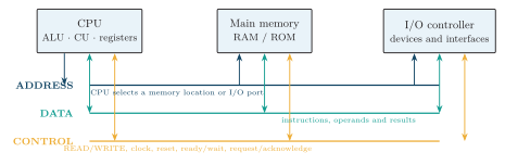
Basic microcomputer organization. The shared system bus comprises a normally CPU-driven address group, a bidirectional data group and a mixed-direction control group.
Von Neumann and Harvard Models
Section titled “Von Neumann and Harvard Models”In a von Neumann architecture, instructions and data share one memory and one transfer path. The design is simple and flexible, but instruction fetches and data transfers compete for the same path, producing the von Neumann bottleneck. A Harvard architecture uses separate instruction and data memories and buses, permitting both accesses at once. Many modern processors use a modified Harvard organization: separate L1 instruction and data caches feed a unified main-memory address space.
| Feature | Von Neumann | Harvard |
|---|---|---|
| Memory | Instructions and data share one space | Separate instruction and data spaces |
| Buses | Common transfer path | Independent instruction and data paths |
| Parallel access | Normally one memory transfer at a time | Instruction and data may be fetched together |
| Main advantage | Simpler hardware and flexible storage | Higher sustained bandwidth |
| Typical use | General-purpose systems | DSPs, microcontrollers and split caches |
Stored-program architecture comparison.
CPU Organization
Section titled “CPU Organization”The central processing unit (CPU) coordinates the computer and executes machine instructions. Its principal units are:
-
Arithmetic logic unit (ALU): performs arithmetic, Boolean, comparison and shift operations.
-
Control unit: decodes the instruction and issues timed register, ALU, memory and I/O control signals.
-
Register set: holds current addresses, instructions, operands, results and processor state at CPU speed.
-
Clock and internal data path: sequence micro-operations and move values among registers and execution units.
| Register | Purpose |
|---|---|
| Program counter (PC) | Address of the next instruction to fetch |
| Instruction register (IR) | Instruction currently being decoded or executed |
| Memory address register (MAR) | Address presented for a memory transaction |
| Memory data register (MDR/MBR) | Word read from or written to memory |
| Accumulator/general registers | Operands and intermediate or final results |
| Stack pointer (SP) | Address of the current top of the runtime stack |
| Status/flags register | Zero, carry, sign, overflow, interrupt-enable and other state bits |
Common processor registers.
Instruction Cycle and Register Transfers
Section titled “Instruction Cycle and Register Transfers”The basic instruction cycle is
For a fixed-length instruction, representative fetch micro-operations are
The control unit then computes any effective address, fetches operands, selects the execution unit and enables the destination register or memory write.
One representative logical instruction layout is
| opcode | addressing mode | destination register | source/register/address field |
|---|---|---|---|
The opcode selects the operation, the mode controls effective-address formation, and the remaining fields identify operands and destinations. The actual field widths and even the number of instruction words are properties of the processor’s instruction-set architecture.
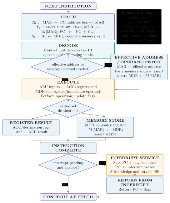
Instruction cycle with explicit CPU register transfers, memory controls, write-back alternatives and interrupt service.
| Phase | Main control action | Possible delay or exception |
|---|---|---|
| Fetch | Read the instruction addressed by PC | Instruction-cache miss |
| Decode | Interpret fields and generate controls | Illegal-opcode trap |
| Operand access | Read registers or calculate and access an effective address | Data-cache/TLB miss or alignment fault |
| Execute | Perform the ALU, branch, memory or I/O operation | Divide fault or branch penalty |
| Write-back | Enable the destination register, memory path and flags | Store buffer or memory wait |
| Interrupt check | Save context and vector to a handler when a request is accepted | A disabled or masked request remains pending |
Instruction phases and representative delay or exception sources.
Interrupts and Pipelining
Section titled “Interrupts and Pipelining”An interrupt requests service for an asynchronous event. If accepted, the CPU completes or precisely records the current instruction, saves the PC and status, loads an interrupt-service address from a vector, services the event, and restores the saved context on return. Interrupts avoid continuous polling, but priority, masking and interrupt latency must be controlled.
Pipelining overlaps stages of successive instructions to increase throughput. It does not necessarily reduce one instruction’s latency. A structural hazard occurs when stages need the same resource, a data hazard when an instruction needs an unavailable earlier result, and a control hazard after a branch or jump. Stalling, forwarding, resource duplication and branch prediction reduce these penalties.