Sequential Logic
A sequential circuit contains memory. Its next state depends on present inputs and the stored present state. A latch is level-sensitive; a flip-flop updates on a clock edge.
Let denote the state before the active event and or the state after it.
Latches
Section titled “Latches”Active-HIGH SR latch
Section titled “Active-HIGH SR latch”Two cross-coupled NOR gates form an active-HIGH set–reset latch. Feedback makes the circuit bistable: after an input pulse ends, the new state remains.
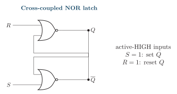
Active-HIGH SR latch made from cross-coupled NOR gates. The feedback paths retain the state after or returns LOW.
| Operation | |||
|---|---|---|---|
| 0 | hold | ||
| 0 | 1 | 0 | reset |
| 1 | 0 | 1 | set |
| 1 | 1 | undefined | forbidden |
Active-HIGH NOR SR-latch operation.
For the valid input combinations,
When , both NOR outputs are forced LOW. Releasing both inputs together can leave the final state dependent on unequal gate delays, so this command is forbidden. A cross-coupled NAND latch instead uses active-LOW inputs and has its forbidden condition at .
A gated SR latch accepts and only while enable is active. A D latch removes the forbidden data combination by applying and through the enable gates. While enabled it is transparent; when disabled it holds the last value.
Flip-Flops
Section titled “Flip-Flops”A flip-flop samples its inputs only around the active clock edge. A triangle at the clock pin denotes edge triggering; a clock bubble plus triangle denotes a falling-edge device.
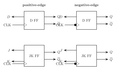
Positive- and negative-edge D and JK flip-flop symbols.
| Type | Input 1 | Input 2 | Next state | Operation |
|---|---|---|---|---|
| SR | hold | |||
| SR | reset | |||
| SR | set | |||
| SR | undefined | forbidden | ||
| JK | hold | |||
| JK | reset | |||
| JK | set | |||
| JK | toggle | |||
| D | – | store 0 | ||
| D | – | store 1 | ||
| T | – | hold | ||
| T | – | toggle |
Characteristic behavior of standard flip-flops.
The characteristic equations are
JK removes the SR forbidden command by making toggle. D is the natural storage element for registers and pipelines. T is convenient for counters and divides clock frequency by two when held at 1.
Excitation table
Section titled “Excitation table”An excitation table works backward from a required state transition to the input that causes it. denotes a don’t-care.
Combined flip-flop excitation table.
Use this table for counter and state-machine design: write present and next states, obtain each flip-flop input, simplify those input functions, then verify legal and unused states.
Triggering
Section titled “Triggering”| Method | When state may respond | Main point |
|---|---|---|
| Level-sensitive latch | Throughout the active enable level | Can be transparent |
| Positive-edge flip-flop | Near the LOW-to-HIGH clock transition | One sample per rising edge |
| Negative-edge flip-flop | Near the HIGH-to-LOW clock transition | One sample per falling edge |
| Master–slave | Master and slave use opposite levels | External output changes once per cycle |
Level and edge control compared.
Race-around and master–slave JK
Section titled “Race-around and master–slave JK”A level-sensitive JK latch with feeds each output change back while the clock remains active. If the active pulse exceeds the feedback round-trip delay, can toggle repeatedly; this is race-around.
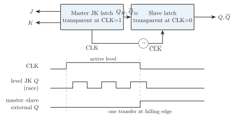
Master–slave JK structure and suppression of external race-around.
The master is transparent during one clock level and the slave during the opposite level. The slave therefore receives one fixed master state and the external output changes once per cycle. A true edge-triggered flip-flop is the usual modern solution.
Setup, hold and clock-to-output delay
Section titled “Setup, hold and clock-to-output delay”-
Setup time : data must be stable for this interval before the active edge.
-
Hold time : data must remain stable for this interval after the active edge.
-
Clock-to- delay : time from the active edge until the output is valid.
Violating setup or hold can place the storage element in metastability: the output may take an unpredictable time to settle. An asynchronous input should normally pass through a synchronizer before entering synchronous logic.
For a register-to-register path, a basic single-clock timing condition is
with a separate minimum-delay check for hold time.
Flip-Flop Applications
Section titled “Flip-Flop Applications”| Element | Typical use |
|---|---|
| SR latch | set/reset control, switch debouncing, simple asynchronous memory |
| D latch | gated data storage and latch-based timing |
| D flip-flop | registers, pipelines, synchronizers and state machines |
| JK flip-flop | counters and flexible state control |
| T flip-flop | divide-by-two stages and binary counters |
Natural applications of each storage type.