Memory
Memory Fundamentals
Section titled “Memory Fundamentals”A semiconductor memory is an addressable array of cells, each storing one bit. Cells are grouped into words; an applied address selects one word for a read or write through decoders, sense/write circuits and data buffers.
| Term | Meaning |
|---|---|
| Memory cell | Smallest element; stores one bit ( or ) |
| Word / word length | Bits accessed together; = bits per word |
| Memory array | Matrix of cells arranged in rows and columns |
| Address lines | inputs that select a word; lines address words |
| Data lines | bidirectional lines carrying one word in or out |
| Control lines | (chip select), (read/write), (output enable) |
Classification
Section titled “Classification”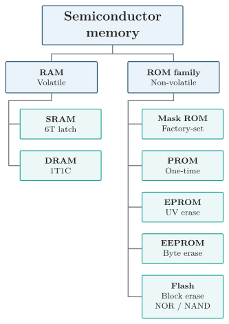
Semiconductor memory types
-
Volatile memory (RAM) loses data when power is removed.
-
Non-volatile memory (ROM family) retains data without power.
-
Read/write memory allows both operations in normal use; read-mostly memory (EPROM, EEPROM, Flash) is programmed by a separate, slower operation.
Memory Organization
Section titled “Memory Organization”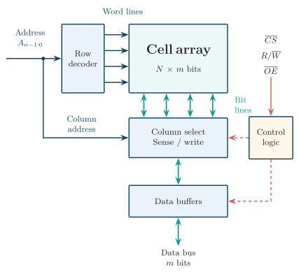
Memory organization
-
The row decoder activates one word line selected by the address.
-
The column decoder with sense and write circuits picks the addressed bits and reads or drives them.
-
Data buffers connect the selected word to the external data bus.
-
The control logic sequences the access from , and .
| Control line | Active | Function |
|---|---|---|
| LOW | Enables the chip; a deselected chip ignores the bus | |
| — | HIGH read, LOW write | |
| LOW | Connects the data buffers to the bus during a read |
Memory Capacity
Section titled “Memory Capacity”where is the number of words, the bits per word and the number of address lines.
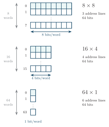
Word organizations
Read Operation
Section titled “Read Operation”-
Place the word address on the address lines.
-
Assert and set (read).
-
Assert ; after the access time the addressed word appears on the data lines.
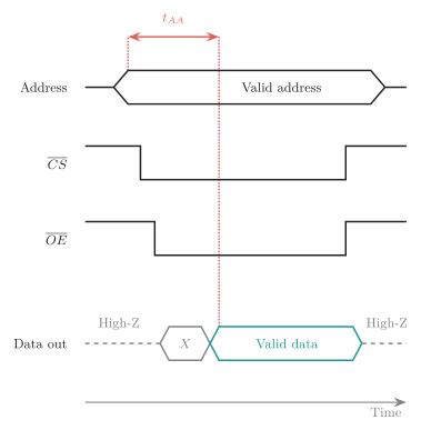
Read-cycle timing
Write Operation
Section titled “Write Operation”-
Place the word address on the address lines.
-
Place the data word on the data lines.
-
Assert and pulse (write); the data is latched on the trailing edge of the write pulse.
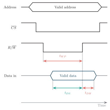
Write-cycle timing
The data must be stable for the setup time before and the hold time after the latching edge; is the minimum write-pulse width.
Random-Access Memory (RAM)
Section titled “Random-Access Memory (RAM)”Random-access memory is volatile read/write memory in which any location is accessed directly in approximately the same time, independent of its address. It holds active programs and data while power is applied.
RAM has two forms that differ in how one bit is stored: SRAM uses a bistable latch, DRAM uses charge on a capacitor.
Static RAM (SRAM)
Section titled “Static RAM (SRAM)”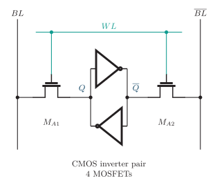
6T SRAM cell
-
Storage: two cross-coupled inverters form a latch that holds the bit while power is present — a 6-transistor (6T) cell (4 latch 2 access transistors).
-
Write: drivers force and to the wanted levels, then is asserted to overwrite the latch.
-
Read: and are precharged; asserting develops a small differential that a sense amplifier resolves. The read is non-destructive.
-
Refresh: not required while powered.
-
Advantages: fast, no refresh. Disadvantages: low density, high cost per bit. Applications: cache, register files, buffers.
Dynamic RAM (DRAM)
Section titled “Dynamic RAM (DRAM)”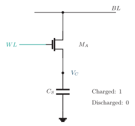
1T1C DRAM cell
-
Storage: one access transistor and one capacitor — a 1T1C cell. A charged is , a discharged is .
-
Write: turns the transistor on and charges or discharges .
-
Read: connecting to the precharged bit line causes charge sharing; a sense amplifier detects the small change and restores the level. The read is destructive, so the cell is rewritten after every read.
-
Refresh: leakage discharges , so every row is refreshed periodically. If rows are refreshed within ,
- Advantages: high density, low cost per bit. Disadvantages: refresh overhead, slower, destructive read. Applications: main memory.
SRAM vs DRAM
Section titled “SRAM vs DRAM”| Parameter | SRAM | DRAM |
|---|---|---|
| Cell | 6T bistable latch | 1T1C charge cell |
| Storage | Flip-flop | Capacitor |
| Refresh | Not required | Required |
| Read | Non-destructive | Destructive (restore follows) |
| Speed | Faster | Slower |
| Density | Lower | Higher |
| Cost per bit | Higher | Lower |
| Main use | Cache | Main memory |
Read-Only Memory (ROM)
Section titled “Read-Only Memory (ROM)”Read-only memory is non-volatile memory whose contents are fixed during manufacture or written once by programming. In normal operation it is read but not written, and it retains data without power.
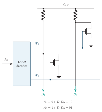
Two-word MOS ROM
Each selected word line reads out a fixed pattern: a cell with a transistor pulls its bit line LOW (), while a cell without one stays HIGH (). The stored data is the pattern of present and absent cells.
| Type | Programming | Erasure |
|---|---|---|
| Mask ROM | During fabrication | Not erasable |
| PROM | Once, by the user (blow fuses) | Not erasable |
| EPROM | Electrical, floating-gate | UV light, whole chip |
| EEPROM | Electrical | Electrical, per byte |
| Flash | Electrical | Electrical, per block |
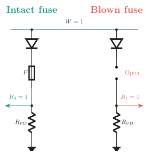
PROM fuse cells
-
Programmable ROM is supplied blank and is programmed once by the user, who irreversibly blows selected fusible links (or forms antifuses).
-
An intact link conducts and reads one logic value; a blown link is open and reads the other. Once programmed it cannot be erased.
-
Applications: permanent low-volume firmware and lookup data.
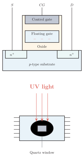
EPROM cell and package
-
Erasable PROM stores each bit as charge trapped on a floating gate. Programming injects electrons with a high voltage, raising the transistor threshold to store a .
-
Erasure exposes the chip to ultraviolet light through a quartz window, which frees the trapped charge and clears the whole chip back to s.
-
It can then be reprogrammed.
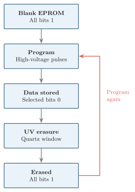
EPROM erase cycle
- Applications: development firmware and reprogrammable fixed data.
ROM vs RAM
Section titled “ROM vs RAM”| Parameter | RAM | ROM |
|---|---|---|
| Operation | Read and write | Read (write only by programming) |
| Volatility | Volatile | Non-volatile |
| Data retention | Lost on power-off | Retained without power |
| Contents set | At run time | At manufacture or programming |
| Main use | Working memory | Firmware, fixed data |
Memory Comparison
Section titled “Memory Comparison”| Feature | RAM | SRAM | DRAM | ROM | PROM | EPROM |
|---|---|---|---|---|---|---|
| Read | ||||||
| Write (normal) | once | |||||
| Volatile | ||||||
| Refresh | — | — | — | — | ||
| Erasable | — | — | — | (UV) | ||
| Relative speed | — | High | Lower | — | — | — |
PROM vs EPROM
Section titled “PROM vs EPROM”| Parameter | PROM | EPROM |
|---|---|---|
| Programmable | Once | Many times |
| Erasable | No | Yes, by UV light |
| Storage mechanism | Fuse / antifuse link | Floating-gate charge |
| Package | Standard | Quartz window |
| Reusable | No | Yes |
Memory Numericals
Section titled “Memory Numericals”Quick Review
Section titled “Quick Review”-
Capacity: words and bits.
-
SRAM: 6T latch, no refresh, fast, low density — cache.
-
DRAM: 1T1C charge cell, destructive read, needs refresh, high density — main memory.
-
ROM: non-volatile; stores a fixed pattern of present and absent cells.
-
PROM: programmed once by blowing fuses; not erasable.
-
EPROM: floating-gate storage; UV-erasable through a quartz window and reprogrammable.