Oscillators
Fundamentals
Section titled “Fundamentals”Oscillator vs Amplifier
Section titled “Oscillator vs Amplifier”An oscillator converts DC-supply power into a periodic AC output without any external periodic input. It contains an active gain element, a frequency-selective feedback network and an amplitude-limiting mechanism. Noise or the switch-on transient supplies the seed; the DC supply—not the feedback network—supplies the energy.
-
Amplifier: needs a periodic input; output amplitude tracks the input; output frequency equals the input frequency.
-
Oscillator: needs no input after start-up; amplitude is set by limiting/AGC; frequency is set by an , or crystal network.
-
An oscillator is essentially an amplifier with positive feedback that regenerates its own input.
| Feature | Amplifier | Oscillator |
|---|---|---|
| Periodic input | Required for a periodic output | Not required after startup |
| Energy source | DC supply, controlled by input | DC supply, controlled by the loop |
| Feedback | Often negative for accuracy and linearity | Regenerative at one selected frequency |
| Frequency | Follows the applied signal within bandwidth | Set by RC, LC or crystal network |
| Amplitude | Proportional to input until limited | Set by AGC or nonlinearity |
| Principal design test | Gain, bandwidth, noise and distortion | Startup, loop phase, amplitude and stability |
Oscillator and amplifier compared.
Positive Feedback
Section titled “Positive Feedback”For forward gain and feedback fraction returned in the reinforcing sense, the loop obeys
A self-sustaining response (input removed) exists when the characteristic equation
has a mode on the imaginary axis.
-
Loop gain is the fraction of output returned per round trip.
-
Feedback must be regenerative (in phase) and selective, so only one frequency is reinforced.
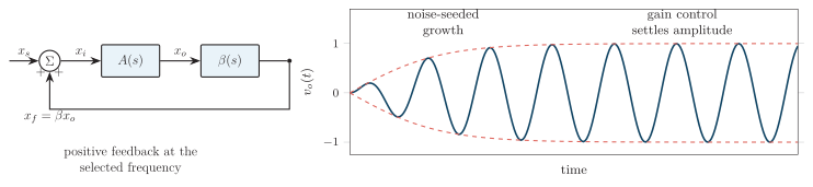
Native oscillator loop and the distinction between startup growth and steady amplitude.
Barkhausen Criterion
Section titled “Barkhausen Criterion”For sustained oscillation at the loop gain must satisfy:
-
Magnitude : the returned signal exactly replaces per-cycle losses.
-
Phase (or ): the returned signal is in phase.
-
Start-up: design so noise grows; amplitude limiting then pulls the average loop gain down to unity:
Amplitude is settled by one of:
-
a lamp or thermistor in the amplifier feedback path;
-
a detector-controlled JFET/OTA or other automatic gain control (AGC);
-
smooth transistor gain compression; or
-
back-to-back diodes/Zeners or another explicit limiter.
Classification
Section titled “Classification”-
By waveform: sinusoidal (, , crystal) or non-sinusoidal / relaxation (multivibrator, UJT, 555 — square, triangular, sawtooth).
-
By frequency-determining network:
-
— Wien bridge, RC phase-shift (audio, low frequency);
-
— Hartley, Colpitts, Clapp (radio frequency);
-
Crystal — Pierce, Miller (very high stability, fixed frequency);
-
Negative-resistance — tunnel diode, UJT (microwave/relaxation).
-
-
By tuning: fixed, variable (VFO) or voltage-controlled (VCO).
| Family | Examples | Typical range | Stability |
|---|---|---|---|
| Wien bridge, phase-shift | – | Moderate | |
| Hartley, Colpitts, Clapp | –hundreds of MHz | Good | |
| Crystal | Pierce, Miller | fixed; kHz–tens of MHz | Excellent |
Sinusoidal oscillator families at a glance.
Resonant Circuits
Section titled “Resonant Circuits”Resonance occurs when inductive and capacitive reactances cancel, leaving a purely resistive terminal impedance. It is the frequency-selecting basis of every oscillator.
Resonant Frequency
Section titled “Resonant Frequency”For ideal , reactance cancellation gives
Series and parallel connections then behave oppositely at .
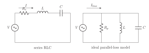
Native series and ideal parallel RLC models. The location of the loss resistance determines the applicable formula.
Series Resonance
Section titled “Series Resonance”With total series resistance ,
-
At : is minimum, current is maximum, power factor .
-
and are equal and opposite, each times the source voltage — voltage magnification.
Half-power points () give , hence
Parallel Resonance
Section titled “Parallel Resonance”For in parallel,
-
At : is maximum, line current is minimum.
-
Equal, opposite reactive currents circulate in the tank — current magnification.
For a practical tank with coil series loss (branch in parallel with ), setting total susceptance to zero gives
For a high- coil, and
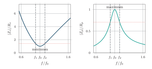
Native normalized response plots for : series impedance has a minimum, while ideal parallel impedance has a maximum.
Q-factor and Bandwidth
Section titled “Q-factor and Bandwidth”; it measures selectivity. Higher means a sharper response and a narrower bandwidth.
-
Half-power bandwidth: for both series and parallel resonance.
-
Higher narrower , sharper selectivity, larger internal / stress, slower settling.
-
Whether a resonator acts band-pass or band-stop depends on where it is inserted and where the output is taken.
| Property | Series resonance | Parallel resonance |
|---|---|---|
| Terminal quantity | minimum, maximum | maximum, minimum |
| Source current | Maximum | Minimum |
| Internal magnification | Voltage across | Circulating current |
| Loss-resistance model | Series | Parallel |
| Typical role | Selective current path, matching | Oscillator/tuned-amplifier tank |
| Lossless limit |
Series and parallel resonance compared.
Wien Bridge Oscillator
Section titled “Wien Bridge Oscillator”Circuit
Section titled “Circuit”-
A non-inverting op-amp with two feedback paths.
-
Positive feedback: a series and a parallel (lead–lag network) to the input — frequency selective.
-
Negative feedback: a resistive divider to the input — sets gain.
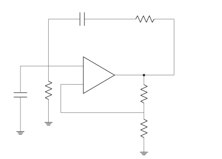
Native op-amp Wien-bridge oscillator with distinct frequency-selective positive feedback and gain-setting negative feedback.
Working
Section titled “Working”-
The lead–lag network gives zero phase shift and maximum transfer at one frequency .
-
There, the amplifier’s plus the network’s satisfy the Barkhausen phase condition.
-
Noise at is reinforced; other frequencies are phase-shifted/attenuated and die out.
Frequency Derivation
Section titled “Frequency Derivation”With and equal components,
The returned fraction is
Zero bridge phase requires .
Gain Condition
Section titled “Gain Condition”For unequal arms (series) and (shunt),
Amplitude Stabilization
Section titled “Amplitude Stabilization”-
Set small-signal gain slightly above 3 so oscillation starts.
-
Lamp/thermistor in the leg lowers gain smoothly toward 3 as amplitude grows — lowest distortion.
-
Back-to-back diodes clamp amplitude — compact but add harmonics.
-
JFET/AGC gives electronic level control over a wide tuning range.
Frequency selectivity: below the series blocks feedback (bridge leads); at the phase is zero and ; above the shunt grounds the node (bridge lags). A convenient audio source with ganged tuning; high-frequency use is limited by op-amp gain–bandwidth and slew rate.
RC Phase-Shift Oscillator
Section titled “RC Phase-Shift Oscillator”-
Circuit: one inverting stage (CE/CS/op-amp) plus a three-section ladder in the feedback path.
-
Working: the amplifier gives and the loaded three-section ladder adds the other at , giving loop phase. ( per section is only a mnemonic — sections load one another.)
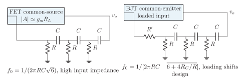
Native FET and BJT forms of the three-section RC phase-shift loop.
For the standard equal-, equal-, unbuffered lag ladder (low-resistance drive, high-resistance input, negligible device capacitance),
-
Set for start-up; limiting brings the average loop gain to unity.
-
Simple and inductor-free, but high attenuation needs high gain, tuning is awkward, and stability/distortion are poorer than a Wien bridge.
Variants (do not mix with the standard formula):
-
an equal-component lead (CR) ladder has under corresponding ideal loading;
-
followers between equal lag sections remove mutual loading, so each section is a true , , and required gain is about 8;
-
a directly loaded single-BJT form gives
| Property | Wien bridge | RC phase shift |
|---|---|---|
| Amplifier | Non-inverting | Inverting |
| Network phase at | combined | |
| Feedback magnitude | for equal parts | under standard assumptions |
| Required gain | steady, slightly above 3 to start | At least 29 to start |
| Tuning/distortion | Convenient ganged tuning; very low with lamp/AGC | Interacting parts; usually higher distortion |
Wien bridge and standard unbuffered phase-shift oscillators.
LC Oscillators
Section titled “LC Oscillators”LC Tank
Section titled “LC Tank”-
Energy oscillates between the capacitor () and inductor () at .
-
Loss would damp the swing; the active device tops up the lost energy from the DC supply each cycle.
Three-reactance criterion. For a lossless three-point tank at :
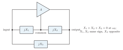
Native general three-reactance oscillator network.
-
Divider arms have the same sign; the third arm the opposite sign.
-
–– Colpitts; –– Hartley.
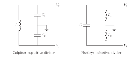
Native Colpitts and Hartley feedback tanks. The labelled voltage terminals define the ratios quoted in the text.
Hartley Oscillator
Section titled “Hartley Oscillator”-
Circuit: tapped inductor () with a single tuning capacitor ; feedback taken from the inductive divider.
-
Working: the tank resonates at ; the coil tap returns in-phase voltage that replaces tank loss and sustains oscillation.
-
Frequency:
- Feedback: for negligible ; the mutual sign follows the coil dots ( aiding, opposing).
Simple one-capacitor tuning, but sensitive to coil loss and mutual coupling.
Colpitts Oscillator
Section titled “Colpitts Oscillator”-
Circuit: single inductor with a capacitive divider ; feedback taken from the capacitor tap.
-
Working: the tank resonates at ; returns in-phase voltage to the device.
-
Frequency:
- Feedback: (the series capacitors carry equal charge); device/stray capacitance adds in parallel with the divider.
Convenient at higher RF; sensitive to device/stray capacitance and loading.
Clapp Oscillator
Section titled “Clapp Oscillator”A Colpitts with a small in series with ; still set the feedback division.
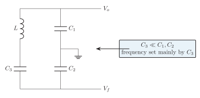
Native Clapp tank: the added series capacitor controls frequency while retain the feedback ratio.
-
A stable dominates the tank, so junction/stray capacitances shift frequency less — better stability than a basic Colpitts.
-
Tuning leaves the feedback ratio nearly fixed, so the start-up margin varies little.
Crystal Oscillator
Section titled “Crystal Oscillator”A crystal oscillator uses a piezoelectric quartz resonator as the frequency-selective element of a feedback loop. Quartz is passive with a very high , so it fixes frequency sharply while the amplifier replaces loss.
Piezoelectric Effect
Section titled “Piezoelectric Effect”-
Direct effect: mechanical stress produces charge/voltage.
-
Inverse effect: an applied voltage produces mechanical strain.
-
An AC voltage excites a natural elastic vibration; the cut (e.g. AT cut) sets the frequency and its temperature behaviour.
Equivalent Circuit
Section titled “Equivalent Circuit”-
Motional arm models loss, vibrating mass and compliance.
-
Electrode/holder capacitance sits in parallel with the whole motional arm.
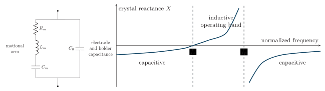
Native quartz equivalent circuit and reactance regions. Impedance is minimum at and maximum near .
Series Resonance
Section titled “Series Resonance”Neglecting , the motional arm is series-resonant when :
At the crystal impedance is minimum (); series-mode oscillators operate here.
Parallel Resonance
Section titled “Parallel Resonance”Above the arm is inductive and antiresonates with . With ,
-
Reactance: capacitive below , inductive only for , capacitive again above .
-
Because , and are very close (– apart).
-
Parallel-mode frequency is set within this window by the external load capacitance.
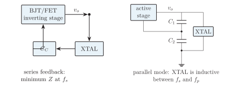
Native series-feedback and parallel-resonant crystal oscillator forms.
In a Pierce network the load capacitance is
The crystal must be specified for series or load-capacitance operation.
Working
Section titled “Working”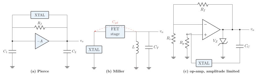
Native crystal oscillator family: Pierce, Miller and op-amp forms.
-
Pierce: inverting FET/CMOS stage () with the crystal and ; a large self-biases the inverter. Standard clock oscillator (fewest parts).
-
Miller: a drain network near antiresonance; gate–drain (Miller) capacitance closes the loop.
-
Op-amp / modified Colpitts: the crystal is the high- element; limiting or a back-to-back Zener clamp can give a square-wave clock.
Stability
Section titled “Stability”-
Very high (–, versus tens–hundreds for an tank) gives a steep phase slope and excellent stability.
-
High stability is not the same as absolute accuracy: frequency still shifts with cut tolerance, temperature, aging, load/stray , supply pulling and drive level.
-
Excess drive heats and ages the crystal (nonlinearity/fracture). Fundamental cut below MHz; odd overtone modes above.
Applications
Section titled “Applications”Microprocessor/clock references, watches, radio carriers, test equipment and frequency synthesisers.
Phase-Locked Loop
Section titled “Phase-Locked Loop”A phase-locked loop (PLL) is a negative-feedback control system that adjusts an oscillator until its divided-output phase tracks a reference phase. In lock, the compared frequencies are equal and the phase error is constant or bounded; the output need not equal the input frequency when a divider is used.
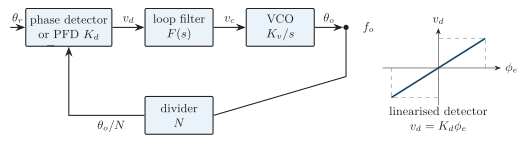
Native PLL with optional divide-by- feedback and a linearised phase detector characteristic.
The phase detector/PFD compares reference and feedback phase/frequency. The low-pass loop filter removes detector ripple and sets bandwidth, damping and acquisition dynamics. The VCO converts control voltage into angular frequency:
Since phase is the integral of frequency, the VCO contributes in the small-signal phase model. Define
Then the linearised reference-to-output phase transfer is
Loop-filter poles and zeros set crossover, damping and phase margin. Wider bandwidth usually gives faster acquisition/tracking but passes more reference and detector noise; narrower bandwidth filters high-frequency input jitter but captures more slowly and tolerates less rapid drift.
Acquisition, lock and ranges
Section titled “Acquisition, lock and ranges”-
Free run: without correction, the VCO runs near .
-
Acquisition: a frequency/phase error creates a varying detector output whose low-frequency component steers the VCO toward the reference-related frequency.
-
Lock: the compared frequencies become equal and a constant phase error supplies the required tuning voltage.
-
Tracking: slow reference or VCO changes create phase error; negative feedback corrects them within loop bandwidth.
For unity feedback,
With divide-by- feedback,
The capture or pull-in range is the set of initial input frequencies from which an unlocked loop can acquire lock under specified conditions. The lock, hold-in or tracking range is the set over which an already locked loop remains locked.
Capture is normally narrower: a large beat frequency is attenuated by the loop filter and must produce a net tuning correction before the phases slip again. Once locked, the detector supplies a DC/low-frequency correction and the loop can often track farther. Exact ranges depend on detector, filter, VCO tuning limits, signal level and acquisition method, so no single range formula applies to every PLL.
PLL applications include programmable frequency synthesis, FM demodulation (the control voltage follows instantaneous frequency deviation), carrier recovery for coherent detection, clock/data recovery, narrowband tracking and jitter/noise filtering. Practical limits include acquisition time, cycle slips or false lock, finite capture/hold ranges, reference spurs, divider/VCO phase noise, tuning nonlinearity and inadequate phase margin.
Comparison
Section titled “Comparison”Wien Bridge vs LC
Section titled “Wien Bridge vs LC”| Feature | Wien bridge () | LC (Hartley/Colpitts) |
|---|---|---|
| Frequency element | and | – tank |
| Typical range | Audio, – | RF, –hundreds of MHz |
| Amplifier | Non-inverting, | Inverting/tuned, gain |
| Waveform purity | Very low distortion (with AGC) | Moderate |
| Inductor | Not needed | Required |
| Tuning | Ganged or | Variable (or ) |
Wien bridge versus LC oscillators.
Hartley vs Colpitts
Section titled “Hartley vs Colpitts”| Feature | Hartley | Colpitts |
|---|---|---|
| Divider | Tapped inductor | Capacitor pair |
| Single element | One capacitor | One inductor |
| Frequency | ||
| Feedback ratio | ||
| Tuning | Simple (one ) | Vary (or add Clapp ) |
| Main weakness | Coil loss, mutual coupling | Stray/device capacitance |
| Typical use | Lower RF | Higher RF, better stability |
Hartley versus Colpitts oscillator.
LC vs Crystal
Section titled “LC vs Crystal”| Feature | LC | Crystal |
|---|---|---|
| Resonator | – tank | Piezoelectric quartz |
| Tens–hundreds | – | |
| Stability | Good | Excellent |
| Tunability | Wide (variable /) | Essentially fixed |
| Cost/size | Low | Higher |
| Typical use | Tunable RF (VFO) | Precise fixed clocks/carriers |
LC versus crystal oscillator.
Formula Validity Map
Section titled “Formula Validity Map”| Topic | Formula or condition | Assumption / validity condition |
|---|---|---|
| Barkhausen | Necessary steady-state loop condition; startup requires and amplitude limiting. | |
| Wien bridge | , , | Equal lead–lag parts and non-inverting amplifier; set gain slightly above 3 to start. General . |
| RC phase shift | , , | Equal unbuffered RC sections with loading included. |
| Colpitts | , | If output is across and feedback across , ; swapped labels invert the ratio. |
| Hartley | , | Mutual sign follows dots. Only for negligible does the labelled ratio reduce to . |
| Clapp | gives ; parasitics are reduced in influence, not eliminated. |
Oscillator formulas with the condition that makes each one valid.
| Topic | Formula or condition | Assumption / validity condition |
|---|---|---|
| Series RLC | , | is total series loss; minimum , maximum line current and voltage magnification at . |
| Ideal parallel RLC | is a parallel loss; maximum finite , minimum line current and current magnification. Lossless is unbounded. | |
| Coil-loss tank | , | High- approximation for series coil loss ; do not confuse with parallel . |
| Crystal series | Minimum impedance of the motional arm; series-feedback oscillators operate near this frequency. | |
| Crystal parallel | Low-loss equivalent circuit. Crystal is inductive only for ; external load capacitance sets the practical parallel-mode frequency. | |
| PLL lock | ; divider: | Only compared frequencies are equal. Capture (pull-in) is normally narrower than hold/lock range; a PLL is a negative-feedback phase-control loop. |
Resonance, crystal and PLL formula map.