Logic Families
A logic family is a set of digital circuits made with one device technology and designed to have compatible supply voltages, logic levels, input/output currents, delay and loading limits.
Parameters Used to Compare Families
Section titled “Parameters Used to Compare Families”| Parameter | Meaning |
|---|---|
| Largest input voltage guaranteed to be interpreted as LOW | |
| Smallest input voltage guaranteed to be interpreted as HIGH | |
| Largest guaranteed LOW output voltage at rated sink current | |
| Smallest guaranteed HIGH output voltage at rated source current | |
| Fan-in | Number of inputs provided by one gate; larger fan-in usually increases delay |
| Fan-out | Maximum compatible inputs that one output can drive in both logic states |
| Output LOW-to-HIGH and HIGH-to-LOW propagation delays | |
| Average power dissipated by one gate under stated static and switching conditions | |
| Noise margin | Allowed unwanted voltage before a guaranteed output can be misread |
Essential logic-family parameters.
The guaranteed noise margins are
For unequal edge delays, quote the average propagation delay
Transistor–Transistor Logic
Section titled “Transistor–Transistor Logic”Transistor–Transistor Logic (TTL) uses bipolar transistors for the input logic decision and for output amplification. The classic 74xx family uses a nominal supply, and its natural primitive is NAND.
Standard TTL NAND gate
Section titled “Standard TTL NAND gate”A two-input TTL NAND contains four functional blocks:
-
multi-emitter input transistor for current steering;
-
phase splitter ;
-
active pull-up with a level-shift diode;
-
pull-down in a totem-pole output.
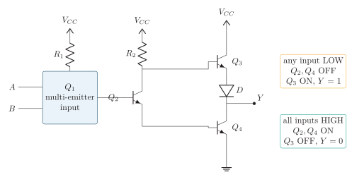
Functional circuit of a standard two-input TTL NAND gate. The integrated multi-emitter device is shown as a labelled current-steering block so its distinct emitter inputs remain legible.
| Inputs | current path | Output stage | ||
|---|---|---|---|---|
| Any input LOW | Current leaves through the LOW emitter | OFF | Pull-up ON, pull-down OFF | |
| All inputs HIGH | Current reaches through | ON | Pull-up OFF, pull-down saturated |
Operation of the standard two-input TTL NAND.
With any LOW input, diverts drive away from ; the output rises. With all inputs HIGH, drives the pull-down and removes pull-up drive; the output falls. Thus .
TTL NOR gate
Section titled “TTL NOR gate”TTL NOR cannot obtain its OR decision from one multi-emitter transistor. It uses a separate input/phase-splitter branch for each input and combines their collector and emitter actions before one output stage.
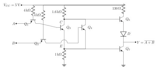
Transistor-level circuit of a two-input TTL NOR gate. Each input has its own current-steering transistor and phase splitter; the splitter collectors and emitters drive the shared – totem-pole output.
| Conducting phase splitter(s) | Pull-down | |||
|---|---|---|---|---|
| none | OFF | |||
| branch | ON | |||
| branch | ON | |||
| both branches | ON |
Two-input TTL NOR state summary.
Any HIGH input activates its branch, lowers the pull-up drive and turns on the common pull-down. NAND is therefore simpler and more economical in TTL.
TTL levels, loading and speed
Section titled “TTL levels, loading and speed”Standard TTL uses guaranteed limits rather than typical values.
| Parameter | Limit | Interpretation |
|---|---|---|
| valid input LOW at or below this value | ||
| valid input HIGH at or above this value | ||
| guaranteed output LOW at rated sink current | ||
| guaranteed output HIGH at rated source current |
Guaranteed standard-TTL voltage limits.
the equation gives
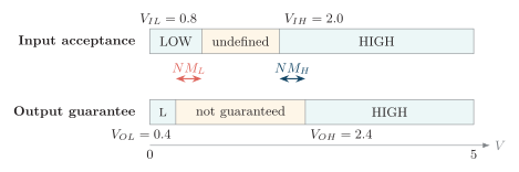
Guaranteed TTL input/output bands and the noise-margin construction.
A LOW TTL output sinks current; a HIGH output sources current. Using current magnitudes,
TTL dissipates static power because bias current flows in either logic state. Deeply saturated BJTs also store charge. A Schottky clamp prevents the base–collector junction from becoming strongly forward biased, reducing storage delay. A common comparison measure is
with units of joules per switching event; lower is better for the stated test conditions.
NMOS Logic
Section titled “NMOS Logic”NMOS logic uses enhancement NMOS transistors in a pull-down network and an always-conducting resistor or depletion-mode MOSFET as the pull-up load. The LOW level depends on the driver-to-load strength ratio.
In a depletion-load inverter the load gate is tied to its source, so . Its threshold is negative, hence it remains ON. The input controls the enhancement NMOS driver.
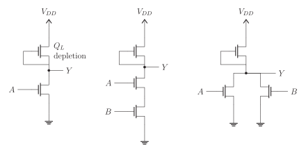
Depletion-load NMOS inverter , NAND with a series PDN, and NOR with a parallel PDN. Each load has its gate tied to source and is always conducting.
| Gate | Pull-down network | LOW-output condition |
|---|---|---|
| Inverter | one controlled NMOS | |
| NAND | NMOS devices in series | every input is 1 |
| NOR | NMOS devices in parallel | any input is 1 |
NMOS primitive-gate operation.
When the driver is OFF, the load charges the output HIGH. When the driver is ON, load and driver conduct simultaneously; a sufficiently strong driver pulls the output LOW. Therefore
The pull-up is weaker than the active pull-down, so LOW-to-HIGH transitions are normally slower than HIGH-to-LOW transitions.
CMOS Logic
Section titled “CMOS Logic”Complementary MOS (CMOS) combines a PMOS pull-up network (PUN) with an NMOS pull-down network (PDN). For every valid stable input, one network should connect the output to a supply rail while the other remains open.
An NMOS turns ON for a sufficiently HIGH gate voltage and naturally pulls toward ground. A PMOS turns ON for a sufficiently LOW gate voltage and naturally pulls toward .
CMOS inverter
Section titled “CMOS inverter”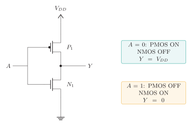
CMOS inverter and its two stable current-path states.
| PMOS | NMOS | Ideal direct path –GND | ||
|---|---|---|---|---|
| ON | OFF | () | open | |
| OFF | ON | (GND) | open |
Static CMOS inverter states.
Near the switching voltage both devices conduct and the output changes steeply. The input thresholds and are conventionally taken where the voltage-transfer curve has slope .
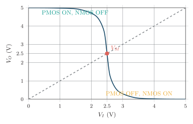
Representative CMOS inverter VTC. The dashed line locates ; its intersection gives the switching point .
The rail-to-rail output and steep transition usually give larger noise margins than standard TTL, but actual limits come from the device data sheet and supply voltage.
CMOS NAND and NOR
Section titled “CMOS NAND and NOR”Build the NMOS PDN from the condition that must pull LOW:
-
AND condition NMOS devices in series;
-
OR condition NMOS devices in parallel.
The PMOS PUN is the dual: replace NMOS by PMOS and interchange series with parallel.
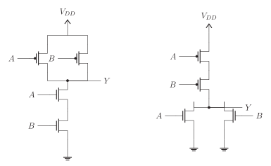
Complementary two-input CMOS networks: NAND uses a parallel PMOS PUN and series NMOS PDN; NOR uses a series PMOS PUN and parallel NMOS PDN.
| Gate | NMOS PDN | PMOS PUN |
|---|---|---|
| NAND | and in series | and in parallel |
| NOR | and in parallel | and in series |
Static-CMOS network rules.
For a complex gate, write the LOW condition , draw the PDN for , then draw its dual PUN. Verify every input row gives one complete rail path and never two stable rail paths.
CMOS delay and power
Section titled “CMOS delay and power”Gate inputs draw negligible steady DC current but add capacitance. Fan-out is therefore limited mainly by charging delay, dynamic energy and leakage rather than by a TTL-like input-current ratio. A first-order estimate is
With switching activity and event rate ,
is the brief short-circuit component while both devices conduct during an edge. Supply reduction lowers dynamic power quadratically, but also reduces noise headroom and drive strength.
CMOS, TTL and NMOS Compared
Section titled “CMOS, TTL and NMOS Compared”| Property | TTL | NMOS | CMOS |
|---|---|---|---|
| Devices | Bipolar transistors | NMOS PDN plus always-on load | Complementary PMOS PUN and NMOS PDN |
| Input loading | Finite DC current | Mainly capacitive | Mainly capacitive |
| Static power | Bias current in both states | High when output is LOW | Ideally leakage only |
| Output swing | Not normally rail-to-rail | Ratio-dependent LOW | Nearly rail-to-rail |
| Fan-out limit | Source/sink current | Capacitance and ratio | Capacitance, delay and leakage |
| Noise margin | Modest, tightly specified | Ratio-dependent | Usually large |
| Typical role | Legacy 74xx control/interface | Historical processors | Dominant modern digital IC technology |
Practical family comparison; exact values depend on sub-family and process.