Combinational Logic
A combinational circuit has no stored state. Its outputs are Boolean functions of the present inputs only. Adders, comparators, multiplexers, demultiplexers and parity circuits are standard examples.
Binary Arithmetic
Section titled “Binary Arithmetic”The elementary addition and subtraction rules are
| Addition | Subtraction | ||||||
|---|---|---|---|---|---|---|---|
| A | B | Sum | Carry | A | B | Difference | Borrow |
| 0 | 0 | 0 | 0 | 0 | 0 | 0 | 0 |
| 0 | 1 | 1 | 0 | 0 | 1 | 1 | 1 |
| 1 | 0 | 1 | 0 | 1 | 0 | 1 | 0 |
| 1 | 1 | 0 | 1 | 1 | 1 | 0 | 0 |
For unsigned -bit addition, a carry beyond bit indicates that the exact result exceeds . For two’s-complement addition, discard that carry and test signed overflow separately.
One’s- and two’s-complement subtraction
Section titled “One’s- and two’s-complement subtraction”To evaluate with one’s complement, add to the bitwise complement of . If a carry leaves the word, add it back to the least-significant bit (end-around carry). Without a carry, complement the sum and mark it negative.
Two’s complement removes the end-around step:
The operation uses the same -bit adder as addition. The result is valid as an -bit signed number only when it lies in .
Adders
Section titled “Adders”Half adder
Section titled “Half adder”A half adder accepts two operand bits but no carry input:
Full adder
Section titled “Full adder”A full adder includes the incoming carry :
| 0 | 0 | 0 | 0 | |
| 0 | 0 | 1 | 1 | 0 |
| 0 | 1 | 0 | 1 | 0 |
| 0 | 1 | 1 | 0 | 1 |
| 1 | 0 | 0 | 1 | 0 |
| 1 | 0 | 1 | 0 | 1 |
| 1 | 1 | 0 | 0 | 1 |
| 1 | 1 | 1 | 1 | 1 |
Full-adder truth table.
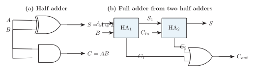
Gate realization of a half adder and construction of a full adder.
Two half adders form a full adder:
Multi-bit ripple-carry adder
Section titled “Multi-bit ripple-carry adder”An -bit parallel adder applies all operand bits together, but each full adder waits for the carry from the next lower position:
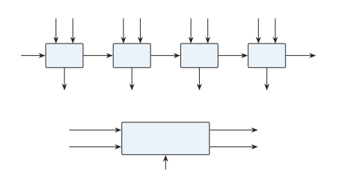
Four cascaded full adders and their compact parallel-adder symbol.
The circuit is regular and economical. Its worst carry path crosses all stages, so a first estimate is
Intermediate sum bits may be temporarily wrong while the carry ripples. A carry look-ahead design instead forms generate and propagate terms so several carries can be evaluated in parallel; it is faster but uses more logic and routing.
Arithmetic Circuits
Section titled “Arithmetic Circuits”Half and full subtractors
Section titled “Half and full subtractors”For a half subtractor,
For a full subtractor with borrow input ,
An ALU normally uses complement addition instead of a separate multi-bit subtractor.
Adder–subtractor
Section titled “Adder–subtractor”Apply mode to every through XOR and also set the initial carry to :
| Operation | |||
|---|---|---|---|
| 0 | |||
| 1 | 1 |
Adder–subtractor modes.
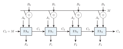
Four-bit adder–subtractor with mode-controlled complementing of .
For two’s-complement arithmetic, signed overflow is
During addition, this is equivalent to equal-sign operands producing an opposite-sign result. The final carry alone is not a signed-overflow flag.
BCD addition
Section titled “BCD addition”First add two BCD digits and the input carry as ordinary binary. If the four-bit sum exceeds 9 or produces carry , add :
For example, gives ; adding produces , the BCD digits 1 and 5.
Digital Comparators
Section titled “Digital Comparators”A magnitude comparator produces mutually exclusive outputs (), (), and ().
One-bit comparator
Section titled “One-bit comparator”| 0 | 0 | 1 | 0 | |
| 0 | 1 | 0 | 0 | 1 |
| 1 | 0 | 1 | 0 | 0 |
| 1 | 1 | 0 | 1 | 0 |
Multi-bit comparator
Section titled “Multi-bit comparator”Compare from the most-significant bit. The first unequal pair decides the result; lower bits matter only when all higher pairs are equal. For two-bit words and , let . Then
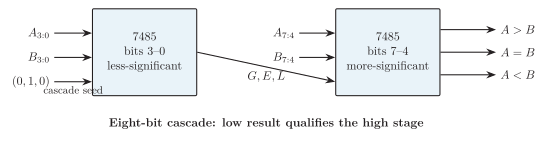
Cascading two four-bit magnitude comparators.
Devices such as the 7485 include cascade inputs. Connect the less-significant group’s outputs to the next more-significant group so the higher group can override lower-bit decisions.
Multiplexers
Section titled “Multiplexers”A -to-1 multiplexer (MUX) uses select lines to connect one of data inputs to one output.
For a four-to-one MUX,
| 0 | ||
| 0 | 1 | |
| 1 | 0 | |
| 1 | 1 |
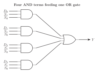
Gate-level realization of a four-to-one multiplexer.
A MUX is also a function generator. For an -variable truth table, connect the variables to the select inputs and each to the required 0 or 1. A -to-1 MUX can implement an -variable function when each data input is chosen from for the remaining variable .
Demultiplexers
Section titled “Demultiplexers”A one-to- demultiplexer (DEMUX) routes one data input to the output selected by address lines. Under the active-HIGH convention used here, all unselected outputs remain 0; practical devices may instead use active-LOW enables or outputs.
For a one-to-four DEMUX,
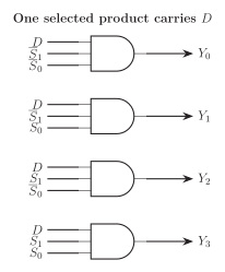
Gate-level realization of a one-to-four demultiplexer.
A decoder with enable acts as a DEMUX when the enable is used as the data input. Check active-LOW enables and outputs on practical devices before applying the active-HIGH equations above.
Parity Generator and Checker
Section titled “Parity Generator and Checker”Parity adds one check bit so the total number of 1s is forced even or odd. For data bits ,
At the receiver, XOR all received data and the parity bit:
For even parity, means parity is consistent and reports an error. For odd parity the interpretation is reversed.
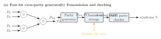
XOR-tree parity generation and end-to-end parity checking.
Combinational Design Checks
Section titled “Combinational Design Checks”-
Verify the Boolean expression against every truth-table row.
-
State active-HIGH and active-LOW conventions explicitly.
-
Check unused input combinations and output exclusivity where required.
-
Count logic levels on the longest path and include fan-out loading.
-
Remember that unequal gate delays can produce temporary hazards even when the final Boolean function is correct.