Analog-to-Digital Conversion
A digital-to-analog converter (DAC) maps an -bit input word to a corresponding analog voltage or current. Its core generates one of finitely many analog levels; an output hold and reconstruction network may then form a continuous-time waveform.
Conversion Chain and Fundamental Quantities
Section titled “Conversion Chain and Fundamental Quantities”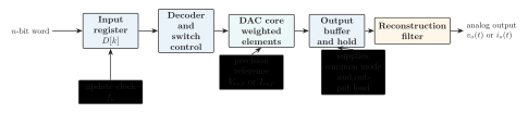
Complete DAC signal path. The core selects an analog level from a digital word and precision reference; buffering, zero-order hold and optional reconstruction filtering determine the delivered continuous-time waveform.
The complete signal path performs three distinct operations:
-
Decode and switch: the registered digital word controls weighted analog elements referred to a precision voltage or current.
-
Generate and buffer: the DAC core produces a voltage or current; an output stage drives the specified load while preserving accuracy and compliance.
-
Hold and reconstruct: each code is normally held until the next update. A low-pass filter suppresses staircase images and switching energy when a smooth waveform is required.
| Quantity | Symbol | Meaning |
|---|---|---|
| Bit depth | Number of input bits; gives possible codewords. | |
| Input code | Integer represented by the applied binary word. | |
| Reference | Precision analog scale from which output weights are derived. | |
| Zero-code output | Output assigned to the minimum code before error is included. | |
| Nominal span | Scale used in the ideal transfer equation. | |
| One LSB / step | Ideal output increment for a one-code increase. | |
| Update rate / period | New words accepted per second and their spacing; . | |
| Settling time | Time after an update to enter and remain in a stated final-value band. | |
| Compliance range | — | Output-voltage interval over which a current DAC or buffer remains accurate. |
| Glitch impulse | Time integral of transient error during a code transition. |
DAC quantities used throughout this section.
Ideal Transfer, Resolution and Coding
Section titled “Ideal Transfer, Resolution and Coding”For unsigned straight-binary code
a common ideal unipolar transfer is
For and ,
The reference is the measuring scale, not generally the supply rail.
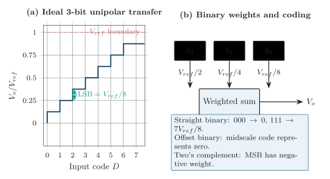
Ideal DAC transfer and binary weighting. An -bit converter has output levels but only intervals between its end codes.
There are output levels but only transitions between end codes:
Thus a unity-scaled unipolar DAC reaches , not . Some data sheets instead call measured endpoint-to-endpoint distance the full-scale range and divide by ; a numerical solution must state the convention used.
For a required nominal step no larger than ,
Each added bit doubles the levels and halves the ideal step at fixed span.
| Coding | Typical endpoint/zero mapping | Interpretation |
|---|---|---|
| Straight binary | minimum; maximum | All bits have positive weights; usual unipolar coding. |
| Offset binary | Midscale | Straight binary shifted by half scale; common bipolar interface. |
| Two’s complement | ; MSB is sign | Signed integer . |
| Thermometer | Number of ones sets level | Adjacent ideal codes switch one unit element; used internally for monotonic MSBs. |
| Gray code | Adjacent words differ by one bit | Reduces simultaneous input transitions but normally requires decoding. |
Common DAC input-code conventions.
For an ideal bipolar two’s-complement DAC with signed integer and bipolar magnitude ,
The most-negative code reaches , whereas the most-positive code is one LSB below . Offset binary gives the same ordered levels after the midscale code is subtracted.
Zero-Order Hold and Reconstruction Filtering
Section titled “Zero-Order Hold and Reconstruction Filtering”A clocked DAC accepts code at update instants and normally holds the corresponding analog level until the next update:
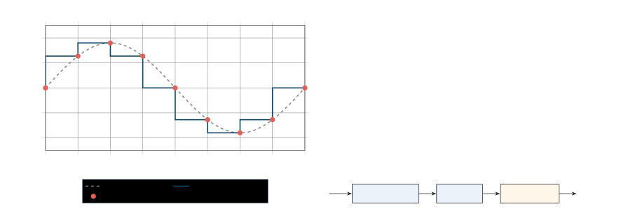
A DAC normally holds each code for one update period . The reconstruction filter passes the wanted baseband and suppresses update images, steps and switching energy; it cannot correct static DAC nonlinearity.
The hold pulse has frequency response
The staircase therefore has sinc amplitude droop and spectral images near integer multiples of . A reconstruction low-pass filter passes the desired baseband and attenuates these images. For baseband bandwidth , choosing leaves a practical filter transition band; oversampling relaxes it.
Update rate, settling time and output bandwidth are different. A DAC may accept codes rapidly yet fail to settle accurately after every full-scale change. Conversely, wide small-signal bandwidth does not guarantee adequate full-scale slew rate.
Static Specifications
Section titled “Static Specifications”Let be settled output and . The actual step is
so
After the stated zero/gain treatment,
where is an endpoint or best-fit reference line.
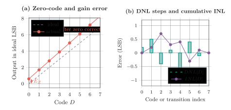
Representative DAC static errors. DNL measures each actual step relative to one ideal LSB; INL measures output departure from a specified straight reference line after the stated offset/gain treatment.
| Specification | Definition | Consequence |
|---|---|---|
| Zero-code error | Nearly constant translation; may consume output headroom. | |
| Offset error | Bipolar zero displacement under stated coding | Creates output at nominal zero code. |
| Gain error | End-scale slope error after zero removal | Error grows with code; reference calibration may reduce it. |
| DNL | Actual step minus one ideal LSB | Determines local step uniformity and monotonicity margin. |
| INL | Output departure from specified straight line | Limits absolute waveform accuracy and creates distortion. |
| Monotonicity | Output never reverses as code increases | Essential in control loops and programmable bias. |
| TUE | Worst unadjusted output error under stated conditions | Combines specified uncalibrated static terms. |
| Temperature drift | Error change, often ppm/C | Sets calibration stability over temperature. |
Principal static DAC specifications.
For an increasing-output DAC,
guarantees nondecreasing output; guarantees every step is positive. A positive DNL above does not itself break monotonicity. A DAC cannot have an unavailable input code; the relevant failure is a zero, reverse or badly sized analog step.
Dynamic and Transition Specifications
Section titled “Dynamic and Transition Specifications”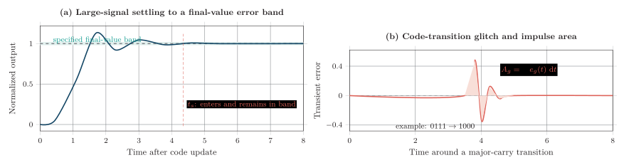
DAC transition behavior. Settling time includes delay, slew and ringing; glitch impulse measures transient error area when internal switches do not change simultaneously.
| Quantity | Meaning | Important distinction |
|---|---|---|
| Update rate | Maximum accepted codewords per second | Does not guarantee full-scale settling at every update. |
| Propagation delay | Input latch to start of output response | Only one component of settling time. |
| Slew rate | Maximum large-signal output slope | Limits rapid large-amplitude transitions. |
| Settling time | Time to enter and remain in stated band | Must name step, load and band, e.g. LSB. |
| Glitch impulse | Integrated transient error at transition | Often worst at major carry such as . |
| Digital feedthrough | Transient without a code change | Couples through switches, package and substrate. |
| Output noise density | Random output noise per | Integrate over effective noise bandwidth. |
| SFDR | Fundamental-to-largest-spur ratio | Captures worst spur, not total noise. |
| THD / SINAD | Harmonic distortion / signal to noise plus distortion | Measures waveform fidelity. |
Dynamic DAC specifications.
Settling contains dead time, slew-limited motion, linear settling and ringing. Crossing final value is insufficient: output must remain in the specified band. Glitch energy comes from unequal switch delay, charge injection and simultaneous bit changes. A deglitching sample-and-hold adds delay, droop and its own noise. For approximately white output-noise density over bandwidth ,
Architecture Families
Section titled “Architecture Families”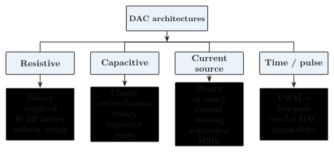
Principal DAC architecture families. Practical ICs often combine families, for example thermometer-coded current-source MSBs with binary LSBs.
No architecture is universally best. Selection depends on resolution, monotonicity, update and settling rate, glitch energy, output type and compliance, static power, silicon area, reference loading and calibration.
Binary-Weighted Resistor DAC
Section titled “Binary-Weighted Resistor DAC”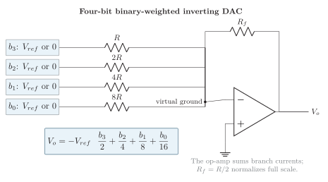
Normalized four-bit binary-weighted resistor DAC. Each switch applies or ground; exponentially increasing branch resistances create the binary current weights.
For branch resistances feeding an ideal virtual ground,
An inverting transimpedance stage gives
Choosing produces the normalized law
The circuit is direct and fast, but an -bit implementation needs resistor values spanning through . Ratio tolerance, switch resistance and parasitic capacitance affect branches unequally; reference current is code-dependent. This makes high-resolution matching and settling difficult.
R–2R Ladder DAC
Section titled “R–2R Ladder DAC”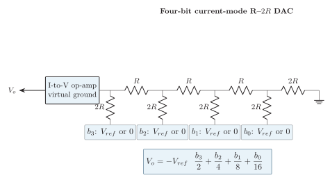
Four-bit R– ladder DAC. Repeating identical sections creates binary weights while requiring only the ratio , which greatly eases matching and IC fabrication.
The termination and every repeated section present the same equivalent resistance when viewed toward the LSB end. Current arriving at each junction therefore divides by two, producing weights . With the shown current-mode polarity and transimpedance scaling,
Only the ratio must match, so process tracking is much better than for an exponential resistor set. Input resistance and switching transients are more uniform, but resistor-ratio error, switch on-resistance, op-amp settling and ladder capacitance still limit high-resolution speed. Voltage-mode ladders can reverse the orientation and buffer a Thevenin output instead of summing current.
Resistor-String DAC
Section titled “Resistor-String DAC”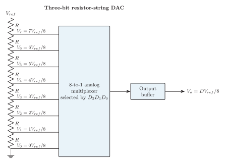
Three-bit resistor-string DAC. A decoder-controlled analog multiplexer selects one of eight ordered taps; positive resistor segments make the ideal architecture inherently monotonic.
A string of equal positive resistors creates ordered taps
A binary decoder and analog multiplexer select tap . Because physical tap voltages remain ordered when all segment resistances are positive, the basic architecture is inherently monotonic. DNL follows individual segment mismatch; buffer offset and switch resistance add code-dependent error.
If each segment is , string current is
Before buffering, tap resistance is approximately
which is largest near midscale. The exponential number of resistors, taps, switches and decoder lines limits resolution, but monotonicity and low glitch make string DACs attractive for trimming, references and display drivers.
Capacitive Charge-Redistribution DAC
Section titled “Capacitive Charge-Redistribution DAC”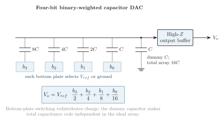
Charge-redistribution capacitor DAC. Binary capacitor ratios replace resistor ratios; CMOS implementations offer negligible static reference current but require accurate capacitor matching and careful switching.
For binary capacitors plus dummy , total capacitance is . Charge conservation after bottom-plate switching gives
for the ideal polarity shown. Capacitors draw essentially no static DC reference current, integrate naturally with CMOS switches and can also sample an input, which is why charge-redistribution arrays dominate SAR ADCs.
The unsplit array area and switching energy grow exponentially with . Capacitor mismatch, parasitic top-plate capacitance, switch charge injection, reference settling and noise limit accuracy. Split or bridged arrays, monotonic switching sequences and calibration reduce area or switching energy.
| Architecture | Main merit | Scaling cost | Dominant limits |
|---|---|---|---|
| Binary weighted | Direct, simple and fast | Resistor spread | Ratio and switch-resistance error |
| R– | Only and ; regular layout | sections | Ratio, parasitic settling, op-amp |
| Resistor string | Inherently monotonic, low glitch | segments and taps | Segment mismatch, mux, tap resistance |
| Capacitor array | Near-zero static current, CMOS friendly | Binary area/energy without splitting | Matching, parasitics, , reference settling |
Comparison of passive-element DAC architectures.
Prevention: (1) place an analog anti-alias LPF before the sampler; (2) set its passband to the wanted signal and attenuate components above ; (3) sample above the theoretical Nyquist rate; (4) leave a guard band for filter roll-off. Once two analog frequencies produce the same sample sequence, no digital filter can separate them.
Oversampling and Undersampling
Section titled “Oversampling and Undersampling”Oversampling () relaxes the analog filter, spreads quantization noise over a wider spectrum and enables digital decimation. Accidental undersampling violates and aliases destructively. Bandpass sampling can sample a narrow RF band below twice its highest carrier if a valid condition is met and a sharp preselector prevents other bands from folding in — this is not permission to violate the Nyquist condition for arbitrary baseband signals.
Telephone speech is limited to , so . Standard telephony uses , giving a Nyquist frequency and a transition band between and .
Sampling Methods
Section titled “Sampling Methods”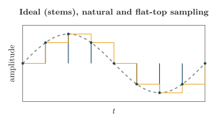
Sampling waveforms: dashed input, ideal impulse samples (stems), and a flat-top (held) staircase; natural sampling would gate the input with finite-width pulses whose tops follow the signal.
Ideal / impulse sampling multiplies the signal by an impulse train : exact values, but a mathematical model. Natural sampling gates the signal with finite-width pulses whose tops follow the input; realizable but the ADC input still changes. Flat-top sampling uses a sample-and-hold to keep one constant value over the aperture — the standard ADC waveform; finite hold width gives a sinc-shaped aperture effect. This predictable passband droop can be corrected when necessary with aperture equalization (inverse-sinc compensation) over the signal band.
| Type | Pulse top | Status | Main issue |
|---|---|---|---|
| Ideal | Zero-width impulse | Model only | Not realizable |
| Natural | Follows input | Realizable | Input still changing |
| Flat-top | Constant held value | Standard ADC | Aperture / sinc droop |
Comparison of the three sampling methods.
Sample-and-Hold Circuit
Section titled “Sample-and-Hold Circuit”A sample-and-hold (S/H) circuit captures the input voltage at a selected instant and holds it nearly constant while the ADC completes conversion.
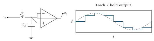
Sample-and-hold: analog switch charges hold capacitor during track, a high-impedance buffer isolates it during hold; the output tracks then holds each sampled value.
-
Sample/track mode: switch closed, charges toward ; output follows the input.
-
Hold mode: switch open, retains charge; the buffer draws little charge through its high input impedance and presents low output impedance to drive the ADC, so .
Why required: an ADC takes finite time to compare and encode. If the input changes during that interval, different bit decisions correspond to different input values; holding removes this dynamic conversion error.
| Specification | Meaning |
|---|---|
| Acquisition time | Time after switch closure to settle within the error band |
| Aperture delay | Delay from sampling command to actual disconnection |
| Aperture jitter | Uncertainty in the sampling instant (critical at high ) |
| Droop rate | Rate the held voltage changes due to leakage |
| Hold step / pedestal | Output jump from switch charge injection at hold |
| Feedthrough | Input/clock coupling to output during hold |
| Settling accuracy | Error band reached before conversion begins |
Sample-and-hold specifications.
For a sinusoidal input, RMS aperture jitter imposes the approximate SNR limit
Quantization
Section titled “Quantization”Quantization maps every held sample to the nearest member of a finite set of amplitude levels.
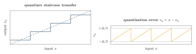
Uniform quantizer: staircase input-output characteristic (top) and bounded by , with resets at the same thresholds (bottom).
With the convention , rounding to the nearest reconstruction level gives the following ideal bounds and mean-square model.
Some data sheets use endpoint spacing ; use the convention stated in the question. Modelling as uniform and uncorrelated gives .
SQNR Derivation for a Full-Scale Sinusoid
Section titled “SQNR Derivation for a Full-Scale Sinusoid”For a bipolar range to : , . Signal power for is , and noise power . Therefore
Every added bit ideally improves SQNR by . A sub-full-scale sine has the same step but less power, so its SQNR falls by the back-off in dB.
Uniform and Nonuniform Quantization
Section titled “Uniform and Nonuniform Quantization”| Feature | Uniform | Nonuniform |
|---|---|---|
| Step size | Constant | Small near zero, larger at high amplitude |
| Concept | Direct uniform ADC | Compressor + uniform ADC, or variable thresholds |
| Weak-signal SQNR | Poorer | Better |
| Main use | General measurement | Speech PCM |
Uniform versus nonuniform quantization.
Companding
Section titled “Companding”Companding combines compression at the transmitter with complementary expansion at the receiver, approximating nonuniform quantization while using a uniform quantizer internally. Speech spends much time at low amplitudes; compression enlarges the relative spacing of weak samples, reducing their fractional quantization error.

Companding chain: compressor and uniform quantizer/encoder at the transmitter; decoder and complementary expander at the receiver.
-law is used in North American / Japanese PCM; A-law in European / international E1 systems. The exact SQNR benefit depends on signal level and implementation; companding redistributes quantization error but does not eliminate quantization noise.
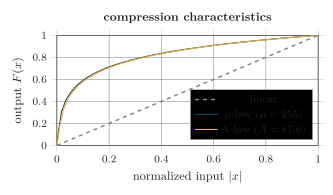
-law and piecewise A-law compression curves: A-law is linear for and logarithmic above ; both enlarge low-level input spacing relative to the linear (dashed) response.
| Feature | A-law | -law |
|---|---|---|
| Parameter | ||
| Region | Europe / international | N. America / Japan |
| Approximation | -segment | -segment |
| Small-signal compression | Slightly less | Slightly greater |
A-law versus -law companding.
ADC Principle and Specifications
Section titled “ADC Principle and Specifications”An ADC compares a held analog value with reference levels and encodes the result as a digital word. For an ideal unipolar converter, the nominal input range is and the unsigned output range is .
Thus clamps to the minimum code, while clamps to the maximum code ; in particular, cannot produce the nonexistent code .
For a sinusoidal test, the standard ENOB relation is
| Specification | Meaning |
|---|---|
| Resolution | One LSB or of full-scale span |
| Conversion time | Time from conversion start to valid output |
| Throughput | Maximum complete conversions per second |
| Offset error | Horizontal shift of the transfer characteristic |
| Gain error | Full-scale slope error measured after offset removal |
| DNL / INL | Code-bin width error / deviation from ideal line |
| Missing code | An output code never produced |
| SNR / SINAD / ENOB | Noise, noise+distortion, effective resolution |
Core ADC specifications.
ADC Architectures
Section titled “ADC Architectures”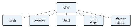
Taxonomy of the five principal ADC architectures.
Flash ADC
Section titled “Flash ADC”An -bit flash ADC uses a resistor ladder, comparators and a priority encoder: the ladder creates all thresholds, comparators compare simultaneously to give a thermometer code, and the encoder produces binary. It is the fastest type (one comparison interval) but comparator count, input capacitance, power and cost grow exponentially — an 8-bit flash needs comparators. Used in oscilloscopes, radar and direct RF/IF sampling.
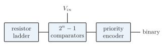
Flash ADC: resistor ladder and a bank of parallel comparators feed a priority encoder.
Counter / Digital-Ramp ADC
Section titled “Counter / Digital-Ramp ADC”A counter from zero drives a DAC; a comparator checks against and counting stops when . Worst case needs clock periods and conversion time depends on input amplitude — simple but slow.
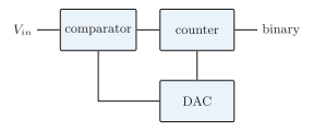
Counter ADC: a counter drives a DAC whose output is compared with in a feedback loop.
Successive-Approximation (SAR) ADC
Section titled “Successive-Approximation (SAR) ADC”A SAR ADC performs a binary search on the held input: the S/H freezes ; the SAR tentatively sets the MSB; the DAC converts the trial code; if the bit is kept, else cleared; the next bit is tested down to the LSB. It takes a fixed cycles regardless of amplitude, giving a strong speed-resolution-power balance (MCUs, instrumentation).
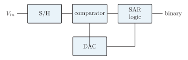
SAR ADC: comparator, feedback DAC and successive-approximation register run an MSB-to-LSB binary search on the held input.
Dual-Slope ADC
Section titled “Dual-Slope ADC”Two integration phases: integrate unknown for a fixed , then apply an opposite reference and count to return to zero.
The result depends on time and reference accuracy, not the absolute ; integrating over whole mains periods gives excellent rejection. Slow — widely used in digital multimeters.

Dual-slope ADC: integrator, zero comparator and control/counter integrate up on then down on .
Sigma-Delta ADC
Section titled “Sigma-Delta ADC”Oversampling far above Nyquist, a feedback loop forcing average 1-bit DAC output to track the input, noise shaping that pushes quantization noise to high frequencies, and a digital decimation LPF removing out-of-band noise. Very high resolution for audio, sensors and precision measurement, with latency.
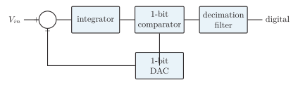
First-order sigma-delta ADC: summing node, integrator, 1-bit quantizer, 1-bit DAC feedback and a digital decimation filter.
| Type | Speed | Resolution | Application |
|---|---|---|---|
| Flash | Very high | Low–med | Oscilloscope, RF DAQ |
| Counter | Low | Medium | Low-cost control |
| SAR | Med–high | Med–high | MCU, instrumentation |
| Dual slope | Low | High | Digital multimeter |
| Sigma-delta | Low BW | Very high | Audio, sensor, precision |
ADC architecture comparison (speed / resolution trade-offs).