Shift Registers
Register Fundamentals
Section titled “Register Fundamentals”A register is a group of flip-flops used to store and manipulate a binary word. An -bit register contains flip-flops, normally driven by a common clock. Depending on its control circuit, data can be loaded, held, shifted, or transferred in serial or parallel form.
A shift register is a register in which the stored bits move from one flip-flop to the next on successive active clock edges.
| Element | Storage capacity | Operation |
|---|---|---|
| Flip-flop | bit | Stores one binary state |
| Register | bits | Stores and transfers one binary word |
| Shift register | bits | Stores a word and shifts it between stages |
Common register controls are:
-
Clock: causes synchronous state changes.
-
Enable or hold: permits a state change or retains the present word.
-
Parallel load: loads all input bits on one active edge.
-
Clear or reset: forces the register to a known state; it may be synchronous or asynchronous.
Four-Bit Shift-Register Principle
Section titled “Four-Bit Shift-Register Principle”Let be the most-significant stage and the least-significant stage. A right shift moves data in the direction
For a four-stage D flip-flop register,
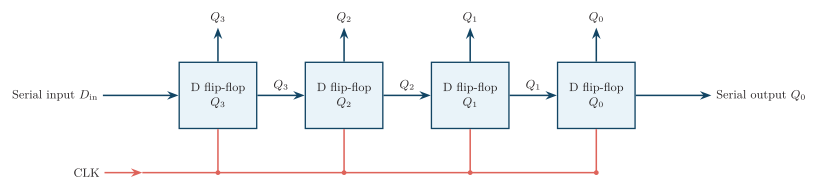
Four-stage D flip-flop shift register with serial path, parallel taps, and common clock
All four flip-flops sample simultaneously. Each next state is determined by the value present at the corresponding D input immediately before the active clock edge.
Clock-by-clock state transition
Section titled “Clock-by-clock state transition”For an initial state and serial input sequence :
| Active edge | after the edge | |
|---|---|---|
| Initial | - | 0000 |
| 1 | 1 | 1000 |
| 2 | 0 | 0100 |
| 3 | 1 | 1010 |
| 4 | 1 | 1101 |
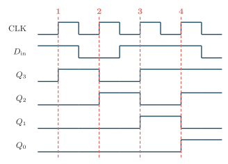
Timing diagram for loading serial sequence 1011 into a four-bit right-shift register
SISO, SIPO, PISO and PIPO Registers
Section titled “SISO, SIPO, PISO and PIPO Registers”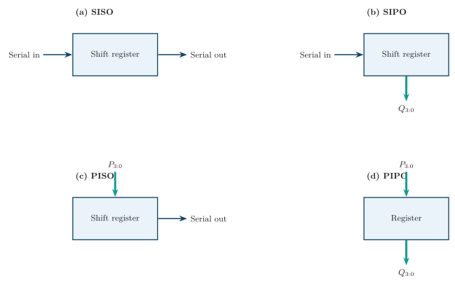
Serial and parallel input-output modes of registers
| Type | Input | Output | Operation | Typical use |
|---|---|---|---|---|
| SISO | Serial | Serial | One bit enters and one bit leaves per clock | Serial delay and serial transfer |
| SIPO | Serial | Parallel | A serial word is shifted in and read simultaneously from all stages | Serial-to-parallel conversion |
| PISO | Parallel | Serial | A word is loaded together and shifted out one bit at a time | Parallel-to-serial conversion |
| PIPO | Parallel | Parallel | A complete word is loaded and read together | Temporary word storage |
Serial-in serial-out register
Section titled “Serial-in serial-out register”In a SISO register, the input stream enters the first stage and passes through every stage. An -stage register requires active edges to fill from an empty state. Once full, one bit enters and one bit leaves on every active edge.
Serial-in parallel-out register
Section titled “Serial-in parallel-out register”A SIPO register uses the same cascaded structure but exposes all outputs . After serial bits have been clocked in, the complete word is available in parallel.
Parallel-in serial-out register
Section titled “Parallel-in serial-out register”A PISO register places a multiplexer before each D flip-flop. Let select parallel load and select right shift:
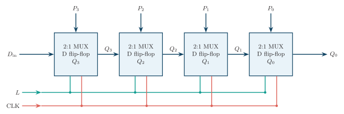
Four-bit PISO register with parallel-load multiplexers and a common clock
One load edge stores . The loaded is the first serial bit; successive shift edges expose the remaining bits at .
Parallel-in parallel-out register
Section titled “Parallel-in parallel-out register”A PIPO register loads all input bits on one active edge and presents all output bits together. With load disabled, feedback from to holds the stored word.
Bidirectional Shift Register
Section titled “Bidirectional Shift Register”A bidirectional shift register shifts either right or left. With serial inputs and ,
Let select right shift and select left shift. A multiplexer before each D input gives
Universal Shift Register
Section titled “Universal Shift Register”A universal shift register performs hold, right shift, left shift, and parallel load. Each stage uses a multiplexer to select its next-state source.
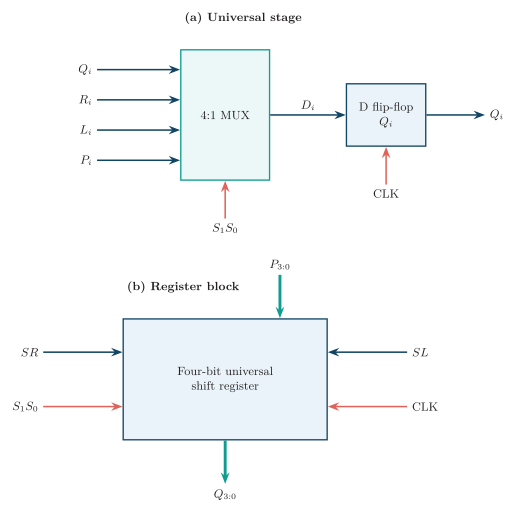
Universal-register stage and four-bit register block
| Selected source | Operation at the active edge | ||
|---|---|---|---|
| Present output | Hold | ||
| Right-shift source | Shift right | ||
| Left-shift source | Shift left | ||
| Parallel input | Parallel load |
The D input of stage is
At the end stages, or is replaced by the corresponding external serial input or .
Logical, Arithmetic and Rotate Operations
Section titled “Logical, Arithmetic and Rotate Operations”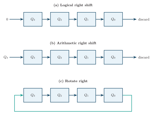
Logical right shift, arithmetic right shift, and rotate-right data paths
| Operation | Next word | Vacated position |
|---|---|---|
| Logical right | Zero enters | |
| Logical left | Zero enters | |
| Arithmetic right | Sign bit is replicated | |
| Arithmetic left | Same bit movement as logical left; signed overflow may occur | |
| Rotate right | returns to | |
| Rotate left | returns to |
For an unsigned word, a logical left shift multiplies by 2 modulo , while a logical right shift gives integer division by 2. Arithmetic right shift preserves the sign of a two’s-complement number.
Timing and Performance
Section titled “Timing and Performance”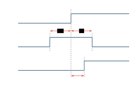
Setup time, hold time, and clock-to-Q delay of a register stage
-
Setup time : minimum interval for which input data must be stable before the active edge.
-
Hold time : minimum interval for which input data must remain stable after the active edge.
-
Clock-to-output delay : time from the active edge until the new output is valid.
For a synchronous register path,
and
All stages use the same clock, so their clock-to-Q delays do not add as when determining . Hold time requires a separate minimum-delay check.
For single-data-rate serial transfer, one bit is accepted per clock period:
A bit captured by the first stage reaches the th stage after further active edges. Its stage-to-stage capture latency is approximately
State-transition example
Section titled “State-transition example”A four-bit register initially contains . Three right shifts apply serial inputs :
| Active edge | Serial input | Bit leaving | New state |
|---|---|---|---|
| Initial | - | - | |
Serial-loading-time example
Section titled “Serial-loading-time example”For an 8-bit SIPO register clocked at ,
Maximum-clock-frequency example
Section titled “Maximum-clock-frequency example”For , , , and ,
Ring and Johnson Counters
Section titled “Ring and Johnson Counters”Ring counter
Section titled “Ring counter”A ring counter is a shift register whose last-stage output is fed directly to the first-stage input:
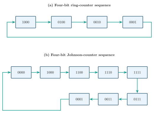
With the one-hot initial state , a four-stage ring counter has the sequence
An -stage ring counter has useful states. It must be initialized with one 1; the all-zero state is locked.
Johnson counter
Section titled “Johnson counter”A Johnson counter, or twisted-ring counter, feeds the complement of the last-stage output to the first stage:
Starting from , a four-stage Johnson counter has the sequence
An -stage Johnson counter has useful states.
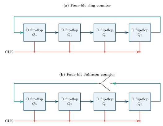
Four-bit ring and Johnson counter circuits
The state-cycle diagram makes the feedback distinction explicit: an -stage ring counter has valid states, whereas a Johnson counter has .
Four-bit ring and Johnson counter state cycles
| Property | Ring counter | Johnson counter |
|---|---|---|
| Feedback | ||
| Useful states with flip-flops | ||
| Normal initialization | Preset one-hot word | Clear to all zeros |
| State pattern | One 1 circulates | 1s fill, then 0s fill |
| Decoding | One stage output per state | Simple two-output decoding |
| Main applications | One-hot timing, scanning, sequence control | Multi-phase timing, frequency division, sequence control |
Standard Shift-Register ICs
Section titled “Standard Shift-Register ICs”| IC | Width and type | Principal controls and features |
|---|---|---|
| -bit SIPO | Serial input, parallel outputs, asynchronous clear | |
| -bit PISO | Parallel load, serial shift input, serial output | |
| -bit universal bidirectional | Hold, shift right, shift left, parallel load |
Applications
Section titled “Applications”| Application | Register operation |
|---|---|
| Serial-to-parallel conversion | SIPO |
| Parallel-to-serial conversion | PISO |
| Temporary word storage and transfer | PIPO |
| Digital delay line | One clock-period delay per stage |
| Arithmetic scaling | Logical or arithmetic shift |
| Bit rotation | Circular feedback |
| One-hot timing and scanning | Ring counter |
| Multi-phase timing | Johnson counter |
| Sequence generation | Feedback shift register or counter-decoder combination |