MOS Transistor Switching Characteristics
A MOSFET is a voltage-controlled, majority-carrier device. An enhancement NMOS is OFF for and conducts when a positive gate overdrive creates an inversion channel. Its insulated gate draws negligible steady current, although gate charge must be supplied at every transition.
Drain Characteristics and Switching Regions
Section titled “Drain Characteristics and Switching Regions”For an enhancement NMOS, neglecting channel-length modulation,
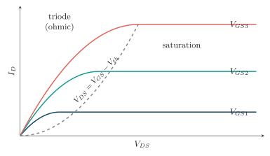
Native MOSFET drain-characteristic family and pinch-off locus; .
| Region | Condition | Switch interpretation |
|---|---|---|
| Cutoff | : open switch; . | |
| Triode | , | Closed switch represented by ; this is the desired steady ON state. |
| Saturation | , | Current-source region, crossed during hard switching and used for amplification. |
For small ,
Resistive-Load Switching Path
Section titled “Resistive-Load Switching Path”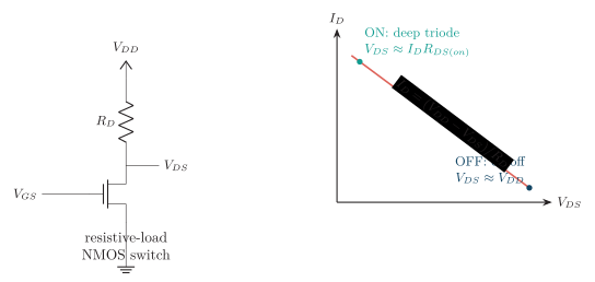
MOSFET switch and its DC load-line endpoints.
Dynamic Switching and the Miller Plateau
Section titled “Dynamic Switching and the Miller Plateau”The gate driver charges and ; the data-sheet input capacitance is . Turn-on occurs in three useful stages:
-
rises to while (delay time).
-
rises to the load current; reaches the plateau level.
-
Gate-drain charge is supplied while falls. This nearly flat part of is the Miller plateau; afterward the gate rises to its final drive voltage.
Turn-off is the reverse sequence. A useful charge-based estimate is ; the simpler RC estimate is .
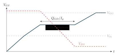
Idealized gate-voltage and drain-voltage turn-on waveforms.
BJT–MOSFET Switching Comparison
Section titled “BJT–MOSFET Switching Comparison”| Feature | BJT | MOSFET |
|---|---|---|
| Control | Base-current controlled | Gate-voltage controlled |
| Carriers | Bipolar; minority charge stored | Unipolar; no minority storage |
| Steady ON state | Saturation, | Deep triode, |
| Dominant delay | Storage time | Gate charge, especially |
| Drive power | Continuous | Dynamic |
| Conduction loss | ||
| Temperature sharing | Thermal-runaway prone | Positive coefficient aids sharing |
| Typical strength | Gain and low fixed ON drop | Fast switching and high integration density |
Integrated MOSFET Fundamentals and Practical Effects
Section titled “Integrated MOSFET Fundamentals and Practical Effects”The switching model is extended here with MOS construction, device types, symbols, static characteristics, circuit operation, second-order effects and a consolidated comparison matrix.
Device Idea, Terminals and Classification
Section titled “Device Idea, Terminals and Classification”A MOSFET is a voltage-controlled, majority-carrier semiconductor device in which an electric field produced by the insulated gate controls the conductivity of a channel between source and drain. Ideally the gate draws no steady DC current; practical gate current is required only to charge and discharge capacitances during transitions.
A MOSFET has four physical terminals:
-
Gate (G): the control electrode, insulated by a thin oxide.
-
Source (S): the terminal from which the channel’s majority carriers enter.
-
Drain (D): the terminal through which those carriers leave.
-
Body or bulk (B): the semiconductor substrate. In most discrete three-terminal MOSFETs the body is internally connected to source.
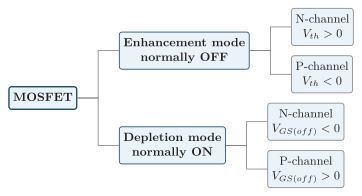
Classification of MOSFETs by channel polarity and operating mode.
Essential Notation
Section titled “Essential Notation”| Symbol | Meaning | Symbol | Meaning |
|---|---|---|---|
| Gate-to-source voltage | Drain-to-source voltage | ||
| Conventional drain current | Threshold voltage | ||
| Overdrive, | Oxide capacitance per unit area | ||
| Channel width-to-length ratio | Channel-length-modulation parameter | ||
| Depletion-device current at | Gate voltage that cuts off a depletion device |
Construction and Channel Formation
Section titled “Construction and Channel Formation”Enhancement NMOS and PMOS Structures
Section titled “Enhancement NMOS and PMOS Structures”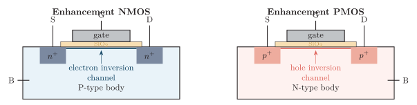
Cross-sections after a sufficient gate voltage has induced a channel. No conducting channel exists at in an enhancement MOSFET.
Formation of the NMOS Inversion Layer
Section titled “Formation of the NMOS Inversion Layer”Consider a positive drain voltage and increase from zero:
-
Accumulation is absent: at , the two regions form reverse-biased junctions with the P-body, so source and drain remain isolated.
-
Depletion: a small positive gate voltage repels holes from the surface, leaving fixed negatively charged acceptor ions.
-
Inversion: a larger positive voltage attracts electrons to the oxide interface. At the surface changes effectively from P-type to N-type.
-
Conduction: for the inversion layer joins source and drain. A positive drives electron flow from source to drain, while conventional flows from drain to source.
For PMOS every semiconductor type and voltage polarity is reversed: an N-body contains source/drain regions, a sufficiently negative creates a hole channel, and conventional current normally flows from source to drain. It is often clearer to use positive magnitudes and for PMOS analysis.
Enhancement and Depletion MOSFETs
Section titled “Enhancement and Depletion MOSFETs”Proper Schematic Symbols
Section titled “Proper Schematic Symbols”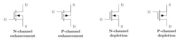
Standard insulated-gate FET symbols drawn with CircuitikZ. A broken channel denotes enhancement mode; a solid channel denotes depletion mode.
Depletion-Mode Operation
Section titled “Depletion-Mode Operation”A depletion MOSFET is fabricated with a physical channel joining source and drain. Consequently it conducts at .
For an N-channel depletion MOSFET:
-
repels electrons and narrows the channel (depletion operation). At , the channel is cut off.
-
attracts additional electrons and raises the current above (enhancement operation).
The P-channel device has all polarities reversed.
Enhancement NMOS Operating Regions
Section titled “Enhancement NMOS Operating Regions”Assume a long-channel enhancement NMOS with body tied to source and define
| Region | Condition | Drain current and meaning |
|---|---|---|
| Cutoff | . No strong inversion channel; the device acts as an open switch. | |
| Triode, linear or ohmic | and | . The channel exists from source to drain and behaves as a voltage-controlled resistance. |
| Saturation or active | and | ideally. The channel pinches off near the drain; current is mainly controlled by . |

Conceptual channel shape in the three NMOS operating regions. In saturation the inversion channel ends before the drain, but the strong electric field carries electrons across the short pinch-off region.
What Pinch-Off Actually Means
Section titled “What Pinch-Off Actually Means”The channel voltage is not constant from source to drain. Let be the local channel potential measured from the source. The NMOS inversion charge per unit area is approximately
It is largest near the source, where , and becomes smaller toward the drain as rises. At the drain end, , so
-
Before pinch-off: When , the bracket remains positive even at the drain. A continuous inversion channel reaches from source to drain, so the MOSFET is in triode.
-
Pinch-off boundary: At , the inversion charge at the drain end becomes zero. In the ideal model the channel tapers to zero at the drain edge; this marks the beginning of saturation.
-
Current does not stop: Electrons travel through the inversion channel to the pinch-off point and are then swept rapidly across the short drain depletion region by its strong electric field. Pinch-off therefore does not mean an open circuit.
-
Beyond pinch-off: Extra falls mainly across the pinch-off region rather than increasing channel charge. The ideal long-channel current is therefore nearly constant at .
At , the triode equation gives the same current as the saturation equation, so the mathematical model is continuous. In a real device, increasing moves the pinch-off point slightly toward the source and shortens the effective channel. This channel-length modulation causes the small upward slope of the saturation curves.
PMOS Region Test
Section titled “PMOS Region Test”Use magnitudes to avoid sign mistakes. For a PMOS define , , and . Then it is:
-
ON when ;
-
in triode when ;
-
in saturation when .
The current magnitude follows the same square-law equations with . PMOS drain-end pinch-off begins at ; holes continue across the high-field region just as electrons do in NMOS, with all polarities and carrier directions reversed.
Static Characteristics
Section titled “Static Characteristics”Drain Characteristics: versus
Section titled “Drain Characteristics: IDI_DID versus VDSV_{DS}VDS”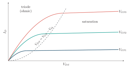
Enhancement-NMOS output characteristics. The small positive slope in saturation represents channel-length modulation; .
At low the device is approximately resistive:
Transfer Characteristics: versus
Section titled “Transfer Characteristics: IDI_DID versus VGSV_{GS}VGS”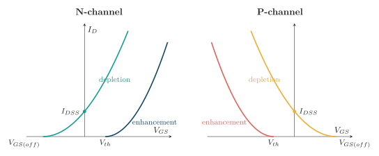
Conceptual transfer characteristics of all four MOSFET types. Current magnitudes are shown for P-channel devices.
MOSFET Circuits
Section titled “MOSFET Circuits”Low-Side NMOS and High-Side PMOS Switches
Section titled “Low-Side NMOS and High-Side PMOS Switches”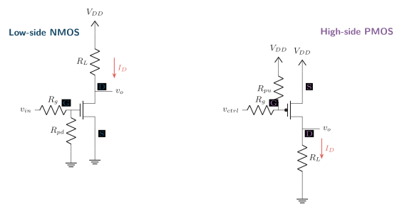
Low-side NMOS switch (left) and high-side PMOS switch (right). , , and identify drain, source, and gate; the red arrow shows conventional current when the switch is ON. and define a safe OFF state when the controller output is floating; limits peak gate current and controls ringing. A HIGH gate drive turns the NMOS ON; a LOW control voltage turns the PMOS ON.
For the low-side NMOS switch:
-
NMOS OFF: , , and .
-
NMOS ON: The driver must provide the data-sheet test gate voltage, not merely exceed . The device operates in deep triode and .
Voltage-Divider-Biased Common-Source Amplifier
Section titled “Voltage-Divider-Biased Common-Source Amplifier”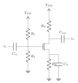
Common-source amplifier with divider bias, source stabilization and an optional AC bypass capacitor .
For negligible gate current,
The bias point must satisfy the saturation test . With effective at signal frequency, the approximate midband gain is ; without bypassing, source degeneration lowers gain but improves linearity and bias stability.
Dynamic Switching and Gate Charge
Section titled “Dynamic Switching and Gate Charge”The insulated gate is not an open circuit during switching. Important capacitances are , and , with . The gate-drain capacitance causes the Miller plateau while the drain voltage changes.
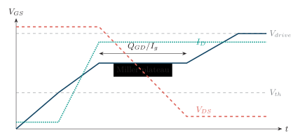
Idealized hard-switching turn-on sequence. rises before falls; their overlap produces switching loss.
-
The driver charges the gate to ; drain current is still nearly zero.
-
Drain current rises to the load current as approaches the plateau voltage.
-
Gate-drain charge is supplied while falls. Gate voltage remains nearly constant at the Miller plateau.
-
After the plateau, the gate reaches its final drive voltage and reaches its specified low value.
Second-Order Effects and Practical Limits
Section titled “Second-Order Effects and Practical Limits”| Effect | Physical result | Practical consequence |
|---|---|---|
| Channel-length modulation | Pinch-off point moves toward source as increases | Saturation curves slope upward; finite lowers amplifier gain. |
| Body effect | Source-body reverse bias raises NMOS threshold | Use . |
| Subthreshold conduction | Weak inversion current remains below threshold | Cutoff current is not exactly zero; leakage matters in low-power ICs. |
| Body diode | Body-source connection forms an intrinsic diode | It conducts reverse current in power circuits and has reverse-recovery implications. |
| Temperature rise | Mobility falls and power-device usually rises | Use hot , thermal resistance and safe operating area. |
| Avalanche and oxide stress | Excess avalanches the drain junction; excess damages oxide | Never exceed absolute maximum ratings; clamp inductive transients and gate spikes. |
Summary and Comparison Matrix
Section titled “Summary and Comparison Matrix”| Property | N-enhancement | P-enhancement | N-depletion | P-depletion |
|---|---|---|---|---|
| At | OFF; no channel | OFF; no channel | ON; channel exists | ON; channel exists |
| Major carriers | Electrons | Holes | Electrons | Holes |
| Gate action | Positive turns ON | Negative turns ON | Negative depletes; positive enhances | Positive depletes; negative enhances |
| Cutoff voltage | $V_{SG}< | V_{tp} | $ | |
| Symbol channel | Broken | Broken | Solid | Solid |
| Usual current direction | D to S | S to D | D to S | S to D |
| Typical use | Low-side switch, CMOS pull-down | High-side switch, CMOS pull-up | Current source, special analog circuits | Less common complementary analog use |
MOSFET versus BJT
Section titled “MOSFET versus BJT”| Feature | MOSFET | BJT |
|---|---|---|
| Control variable | Gate voltage and gate charge | Base current |
| Carrier mechanism | Majority-carrier, unipolar | Both carrier types, bipolar |
| Input resistance | Extremely high at DC | Finite because base-emitter junction conducts |
| Steady ON model | in deep triode | in saturation |
| Dynamic limitation | Gate and Miller charge | Stored minority charge and base charge |
| Conduction loss | Approximately | |
| Thermal sharing | Positive coefficient often helps | Thermal runaway is more problematic |