A/D Converters
An analog-to-digital converter (ADC) samples a continuous input, assigns each sample to one of a finite number of amplitude levels (quantization), and encodes that level as a binary word. A complete data-acquisition path therefore uses anti-alias filtering, sampling/holding, quantization and encoding.
ADC Language, Conversion Chain and Ideal Transfer
Section titled “ADC Language, Conversion Chain and Ideal Transfer”
A complete ADC signal path: sampling discretizes time, quantization discretizes amplitude, and encoding expresses the selected level in binary.
The three conversion operations are distinct:
-
Sampling: selects values at and therefore discretizes time; .
-
Quantization: maps each held value to one of amplitude intervals and is the irreversible step.
-
Encoding: labels the selected interval with an -bit binary word; it introduces no additional ideal error.
Fundamental quantities and vocabulary
Section titled “Fundamental quantities and vocabulary”| Quantity | Symbol | Definition |
|---|---|---|
| Analog input | Continuous-time voltage presented to the ADC front end. | |
| Sample | Input value selected at sampling instant . | |
| Sampling rate/period | Samples requested per second and their spacing; . | |
| Bit depth | Number of binary digits in one output codeword. | |
| Number of codes | Distinct digital words, numbered through . | |
| Input limits | Lowest and highest specified analog inputs. | |
| Full-scale span | Width of the input range: . | |
| Reference | Precision voltage that establishes the converter scale; for a simple unipolar ADC, . | |
| Step size / 1 LSB | Ideal width of one code bin in volts: . | |
| Code / codeword | Integer bin index and its -bit representation. | |
| Transition voltage | Input boundary at which the output changes from code to . | |
| Code bin | — | Input interval producing one code; ideal width is . |
| Quantized estimate | Analog value assigned to the selected code, often its bin midpoint. | |
| Quantization error | Difference caused by finite amplitude bins. | |
| Clipping / overrange | — | Input lies outside the allowed span, so the output remains at an end code. |
ADC quantities used throughout this chapter.
Resolution in detail
Section titled “Resolution in detail”The bit depth fixes the number of available codewords, . The word resolution may mean bit depth, one ideal LSB in volts, or the fractional step of full-scale span. It describes granularity, not total measurement accuracy.
Thus resolution may be reported in three equivalent ideal forms:
Let be the allowed input span. For an ideal -bit uniform ADC,
The nominal, non-overload range is the half-open interval ; values outside it, including , saturate at an end code. If code represents the midpoint of its interval, then, within the nominal range,
The variance model assumes no overload and quantization error that is approximately uniform and uncorrelated with the input, as occurs for a sufficiently active or dithered signal. For DC or coherent low-level inputs, the error can instead be deterministic and correlated. Bipolar and offset-binary converters use the same span rule with a shifted code origin. Datasheets occasionally quote endpoint spacing , so the convention stated in a numerical problem must be followed.
Resolution answers the ideal question, “how finely is the selected input span divided?” It depends on both bit depth and span:
-
increasing by one doubles the number of codes and halves ;
-
keeping fixed but narrowing also reduces , although it reduces allowable input headroom and may cause clipping;
-
widening a bipolar range means using its complete span. For example, a range has , not .
For a required ideal voltage increment , the minimum bit depth is
This calculation selects nominal granularity only. Noise, DNL, INL, offset, gain and reference uncertainty determine whether such a small input change can actually be distinguished or measured accurately.
| Term | Meaning |
|---|---|
| Nominal resolution | Ideal code count or code-bin width: codes and . |
| Accuracy | Closeness of the reported value to the true input after systematic and random errors. |
| Effective resolution/ENOB | Usable dynamic resolution inferred from measured noise plus distortion, generally less than . |
| Noise-free resolution | Stable code divisions remaining after peak-to-peak code flicker or transition noise. |
| Sensitivity | Smallest input change producing a reliably observable output change under stated test conditions. |
Meanings that must not be confused with nominal resolution.
Reference voltage in detail
Section titled “Reference voltage in detail”The reference voltage is the precision analog standard against which the sampled input is compared. It establishes the converter’s transfer scale: its value determines the ideal transition voltages and therefore the number of input volts represented by one code.
The reference is the ADC’s measuring ruler; it is not simply the supply voltage. The analog supply powers the circuitry, whereas the reference defines the scale. Some ADCs contain a factory-trimmed internal reference, some require an external reference, and others permit either. In every case the input, reference and supply pins must obey the ranges stated in the datasheet.
For a common unity-scaled unipolar ADC with ,
More generally, a converter may use positive and negative reference pins, internal scaling or bipolar input translation. A useful model is
where its datasheet defines . Therefore only in the simple unity-scaled case.
Changing the reference does not create more digital codes: an -bit ADC still has codewords. A lower permitted reference reduces volts per code but also reduces input headroom, and makes fixed input noise and offset larger when expressed in LSBs. In the simple unipolar model the last code covers ; is the upper range boundary, not an additional code value.
Away from clipping, the ideal code is proportional to . Thus a small reference change has opposite signs depending on what is held fixed:
A higher actual reference therefore produces fewer codes for the same input, while a fixed code represents more volts.
| Reference property | Effect on conversion |
|---|---|
| Initial accuracy | A constant reference-ratio error produces a full-scale or gain error. |
| Temperature coefficient | Drift in causes the transfer scale to move with temperature. |
| Noise | Moving thresholds cause code flicker and reduce SNR, SINAD and ENOB. |
| Output impedance | Dynamic ADC reference current can disturb the voltage at the reference pin. |
| Settling/load recovery | Incomplete recovery can create signal- and code-dependent conversion error. |
| Long-term drift | Calibrated gain changes over months or years. |
| Bypass network | Local charge storage supports transients; poor placement or unsuitable capacitance increases error. |
Reference properties and their ADC consequences.
An internal reference simplifies design, while an external one can offer a different range, noise or drift grade. Either must satisfy the specified drive and decoupling requirements. A ratiometric system excites a sensor and references the ADC from the same source. If , then
so common slow reference changes cancel from the ideal code ratio. This does not cancel reference noise, settling error, offset or nonlinearity.
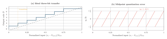
Ideal uniform ADC model. Each horizontal code bin has width ; midpoint reconstruction produces a bounded sawtooth error over the nominal half-open range. The point at is clipped to the top code.
Common output coding conventions
Section titled “Common output coding conventions”| Coding | Typical range and zero code | Interpretation |
|---|---|---|
| Straight binary | Unipolar; is the minimum input | All bits have positive weights. |
| Offset binary | Bipolar; midscale represents zero | Straight binary shifted by half scale. |
| Two’s complement | Bipolar; represents zero | MSB has negative sign weight; convenient for arithmetic. |
| Gray or thermometer code | Internal high-speed stages | Adjacent states change minimally; translated before normal binary output. |
Common ADC code conventions.
Sampling, Anti-Aliasing and Sample-and-Hold
Section titled “Sampling, Anti-Aliasing and Sample-and-Hold”The sampling rate is the number of sampling instants per second; the sampling period is . The signal bandwidth is the highest baseband frequency that must be preserved. The Nyquist rate is , whereas the Nyquist frequency for an already chosen is .
An ideally band-limited baseband input can be reconstructed if
Sampling replicates the analog spectrum around integer multiples of . Aliasing occurs when these replicas overlap, making different analog frequencies produce the same samples. A sinusoid at appears in the first Nyquist zone at
where integer is chosen to place in that interval. Because aliasing is irreversible after sampling, a realizable analog anti-alias low-pass filter and a guard band require in practice.
Sampling rate in detail
Section titled “Sampling rate in detail”Sampling rate determines how closely samples are spaced in time; it does not determine amplitude resolution. At samples per second, adjacent ideal aperture instants are apart. A sinusoid at is represented by
samples per cycle. Increasing this ratio gives a denser time record and can ease waveform processing, but it neither adds nominal ADC bits nor removes analog errors by itself.
The Nyquist inequality is a mathematical lower bound for an ideally band-limited signal, not a complete hardware design rule. Equality leaves no transition band for a realizable anti-alias filter and can sample a band-edge tone at an unfortunate phase. In practice one chooses , passes the wanted band to , and attenuates unwanted analog content before it can fold into that band. The oversampling ratio is
An provides filter guard band. With suitable digital low-pass filtering and decimation, oversampling can also reduce in-band white noise. Merely collecting more noisy samples without filtering does not guarantee higher accuracy.
| Quantity | Meaning |
|---|---|
| Sampling rate | Aperture instants per second; it sets and the Nyquist frequency . |
| Throughput/output rate | Completed codewords delivered per second; it may differ from sampling rate. |
| Conversion clock | Clock used for internal bit decisions; several cycles may be required per sample. |
| Conversion time | Time the architecture needs to determine one sampled code. |
| Latency | Delay from one sample’s aperture instant until that sample’s code appears. |
| Analog input bandwidth | Front-end frequency range that can reach the sampler, not the unaliased baseband limit. |
| Per-channel sample rate | Rate seen by one channel; in an -channel scan it is at most roughly aggregate rate/. |
Rates and bandwidths often confused in ADC specifications.
Architecture and acquisition impose an additional upper limit. A basic SAR conversion cycle must provide time to acquire and convert,
A pipeline ADC can deliver one result each clock after a multi-cycle latency; a sigma-delta modulator samples internally much faster than its decimated output-word rate. After a multiplexer changes channel, the driver and sampling capacitor must settle again, so usable per-channel rate can be lower than the simple aggregate-rate division.
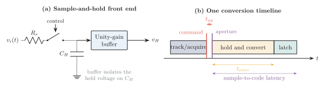
Sample-and-hold circuit and timing vocabulary. Aperture delay locates the actual sampling instant; latency extends until the corresponding code is valid.
| Quantity | Definition | Why it matters |
|---|---|---|
| Track mode | Switch closed; follows the input | Driver must charge the ADC input network. |
| Acquisition time | Time to settle after entering track mode | Limits source resistance and multiplexing speed. |
| Aperture delay | Mean delay from sample command to actual hold instant | Shifts the effective sampling time. |
| Aperture jitter | Random uncertainty of the aperture instant | Converts input slew into voltage noise. |
| Droop rate | Held-voltage change caused by leakage | Creates error during a long conversion. |
| Hold step/pedestal | Output jump at track-to-hold transition | Caused mainly by switch charge injection. |
| Feedthrough | Input or clock coupling into the held node | Disturbs the supposedly constant sample. |
| Settling accuracy | Error band reached during acquisition | Must normally be below the allocated LSB fraction. |
Sample-and-hold quantities.
For a simple first-order source resistance charging input capacitance , settling from a full-scale step to within LSB requires approximately
Real ADC data sheets include switch resistance, charge redistribution and driver recovery, so this is a design estimate rather than a replacement for the specified acquisition-time test.
ADC Specifications and Error Terms
Section titled “ADC Specifications and Error Terms”ADC quality is described in three complementary ways: static transfer tests use slowly changing or DC inputs; dynamic tests use sampled sinusoids and spectra; timing/interface tests describe when a valid code appears and how quickly another conversion can begin.
Static transfer specifications
Section titled “Static transfer specifications”| Specification | Meaning or relation | Design consequence |
|---|---|---|
| Resolution | bits, codes; | Ideal granularity, not guaranteed accuracy |
| Input range/span | Allowed limits and | Must match signal, common-mode and reference limits |
| Transition voltage | Input at which one code changes to the next | Basic measured point for transfer testing |
| Quantization error | Ideally bounded by for midpoint rounding | Irreducible ideal amplitude uncertainty |
| Offset error | Horizontal shift of transfer characteristic | Produces nearly constant code error |
| Gain error | Full-scale slope error after offset removal | Reference/gain calibration can reduce it |
| DNL | Actual code width minus | DNL prevents missing codes |
| INL | Deviation from an ideal straight transfer line | Limits absolute accuracy and distortion |
| Monotonicity | Code never decreases as input increases | Essential in control and closed-loop systems |
| Missing code | A nominal code has no positive-width input bin | Indicates local non-monotonic or zero-width behavior |
| Transition noise | Code spread under repeated conversion of one DC input | Sets code flicker and noise-free resolution |
| TUE | Worst total unadjusted error under stated conditions | Combines specified uncalibrated error contributions |
| Reference and temperature drift | Change of scale and errors with supply/temperature | Sets long-term calibration stability |
Static ADC specifications.
Define endpoint boundaries and , where ; for , let be the actual transition from code to . The width of code , , is . Then
INL must name its reference line (endpoint or best fit). A code is missing when , equivalently LSB. If the peak-to-peak input-referred transition noise is , an approximate noise-free resolution is
provided the measurement bandwidth and test method are stated.
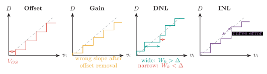
Static ADC errors relative to the dashed ideal transfer. Offset and gain change scale; DNL changes code widths; INL measures transfer curvature.
Offset and gain errors in detail
Section titled “Offset and gain errors in detail”Offset error
Section titled “Offset error”Offset error translates the transfer characteristic horizontally without ideally changing the spacing between transitions. Using the transition-voltage sign convention adopted here,
A positive value means the measured transition occurs at a larger input voltage (the staircase is shifted right). Some data sheets define polarity from code error rather than transition error and therefore reverse this sign; the stated convention must always be checked.
Applying zero input and observing a nonzero code is a useful quick test only for a compatible unipolar coding convention. Measuring the first specified transition is the more general definition. Digital subtraction can calibrate offset, but cannot recover analog headroom already lost by early clipping.
Gain error
Section titled “Gain error”Gain error is measured after offset removal. It changes the average slope or span of the transfer. One transition-based definition is
Here “corr” means that the measured characteristic has first been translated to remove offset. A two-point calibration can correct offset and average gain, but any curvature, unequal code widths, noise and clipping remain.
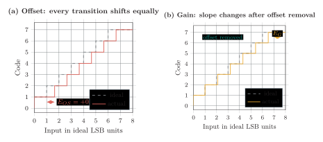
Offset and gain errors measured from transition positions. Offset is removed first; gain error is then measured at the upper end of the transfer.
DNL, missing codes and monotonicity
Section titled “DNL, missing codes and monotonicity”Differential nonlinearity is a local width error. If one measured code bin has width , then LSB; if , then LSB. At , LSB and code is missing.
INL and its relation to DNL
Section titled “INL and its relation to DNL”Integral nonlinearity is a global transition-position error. Before removing endpoint slope, the transition locations satisfy
when the same and ideal are used. Thus consecutive positive or negative DNL values accumulate into INL; isolated positive and negative DNL can partly cancel.
Two reference-line methods are common:
-
Endpoint INL: Use the line through specified end transitions after offset/gain handling. It preserves endpoint meaning and is common in precision specifications.
-
Best-fit INL: Choose a regression line that best fits all measured transitions. It usually reports a smaller numerical INL, so values from the two methods are not directly interchangeable.
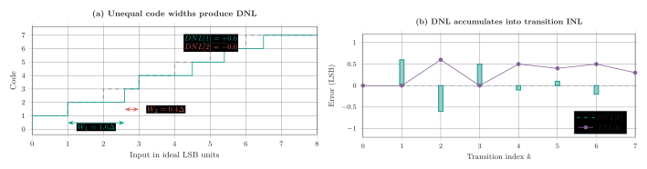
Differential and integral nonlinearity. DNL measures each bin width; transition-based INL is the cumulative departure from the chosen ideal line.
Timing and dynamic specifications
Section titled “Timing and dynamic specifications”| Quantity | Definition | Important distinction |
|---|---|---|
| Sampling rate | Sampling instants requested per second | Must satisfy anti-alias needs. |
| Throughput/output rate | Completed output words per second | Can differ from or inverse latency. |
| Conversion time | Time used internally to determine one code | Architecture dependent. |
| Latency | Delay from aperture instant to corresponding valid output | A pipeline may have high throughput but many-cycle latency. |
| Analog input bandwidth | Front-end frequency response before sampling | May exceed ; does not permit unplanned aliasing. |
| SNR | Fundamental signal power divided by noise power | Excludes harmonic distortion. |
| SINAD | Fundamental divided by noise plus distortion | Directly determines ENOB. |
| THD | RSS harmonic rms amplitude divided by fundamental amplitude | Measures nonlinearity, not random noise. |
| SFDR | Fundamental-to-largest-spur ratio | Does not integrate the entire noise floor. |
| ENOB | Equivalent ideal bit count from measured SINAD | Dynamic performance, usually frequency dependent. |
| Aperture jitter | RMS sampling-time uncertainty | Sets an SNR limit that worsens with . |
Timing and AC specifications.
For an ideal full-scale sinusoid and uncorrelated uniform quantization error,
while sampling-clock jitter imposes approximately
This assumes an ideal ADC and sufficiently active codes; real SINAD also contains thermal noise, clock jitter, harmonic distortion and reference error. Resolution is therefore not the same as accuracy or effective resolution.
ADC Architecture Families
Section titled “ADC Architecture Families”An ADC architecture is the internal method used to locate the input’s code bin. Parallel comparison minimizes decision time; feedback methods reuse one comparator; subranging resolves a few bits per stage; integration converts voltage to a time ratio; oversampling trades excess sample rate for in-band resolution.
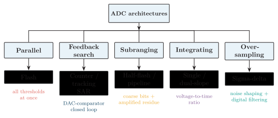
Principal ADC families organized by the mechanism used to reach a code.
No architecture is universally best. Selection starts with signal bandwidth, required ENOB, latency, throughput, power, input loading, noise rejection and whether deterministic timing or absolute DC accuracy matters most.
Unless stated otherwise, the architecture equations and numerical examples below use a unipolar straight-binary range with and . Bipolar designs shift the origin or select reference polarity according to their coding.
Flash (Parallel) ADC
Section titled “Flash (Parallel) ADC”A Flash converter generates all decision thresholds with a resistor string, compares the sampled input with every threshold simultaneously, and converts the resulting thermometer code to binary with a priority encoder. An -bit converter requires
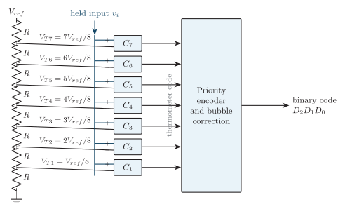
Three-bit Flash ADC: the ladder creates seven thresholds, the comparator bank produces a thermometer code, and the encoder returns a three-bit word.
| Input interval | Comparators HIGH | Thermometer code | Binary output |
|---|---|---|---|
| none | |||
| – | |||
| – | |||
| – | |||
| – | |||
| – |
Complete three-bit Flash conversion table; comparator order is , from highest to lowest threshold.
At an exact ideal threshold either adjacent code can appear depending on the specified transition convention; comparator offset and noise create a small real uncertainty region. Writing comparators in ascending order reverses every thermometer word, so the ordering must always be labelled.
All decisions occur in parallel, so Flash is the fastest architecture, requiring essentially one comparator-plus-encoder delay. The cost is exponential area, power and input capacitance: 8 bits require 255 comparators and 10 bits require 1023. Comparator offset, resistor mismatch and metastable “bubbles” limit accuracy, so Flash is normally low/medium resolution. Applications include oscilloscopes, video, radar and very-high-speed data acquisition.
Operating sequence and practical circuitry
Section titled “Operating sequence and practical circuitry”-
Acquire and hold so every comparator sees the same voltage.
-
The equal ladder resistors create thresholds .
-
All comparators resolve simultaneously. With for , the ideal outputs form one monotonic run.
-
Bubble-correction logic removes sparse isolated comparator errors.
-
A leading-one/priority encoder finds the highest crossed threshold and latches its index as the binary output.
Practical comparator channels often contain a low-offset preamplifier, a fast regenerative latch and a retiming register before the encoder. Preamplification reduces latch kickback and input-referred offset; retiming aligns unequal comparator delays and confines metastability before deep logic.
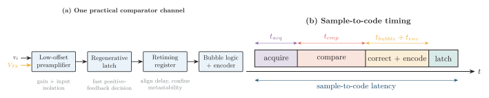
A practical Flash comparator path and its latency components. Extra register stages can raise throughput but add clock-cycle latency.
With acquisition excluded from the internal decision time,
An unpipelined converter’s maximum output rate is limited by this cycle. A registered or pipelined comparator/encoder tree may sustain a higher throughput while adding one or more clock cycles of latency.
If every resistor-string segment has resistance ,
If a fixed total resistance is chosen instead, each segment is and . The signal driver sees roughly
so comparator input capacitance and kickback also grow exponentially.
| (bits) | 3 | 4 | 6 | 8 | 10 |
|---|---|---|---|---|---|
| Codes/resistors | 8 | 16 | 64 | 256 | 1024 |
| Comparators | 7 | 15 | 63 | 255 | 1023 |
Full-Flash hardware growth.
Bubbles and metastability
Section titled “Bubbles and metastability”An ideal thermometer code has only one zero–one boundary. Comparator offset, noise, reference kickback, unequal delay or input motion can create an isolated wrong bit called a bubble. Local majority logic such as
can repair a sparse one-bit bubble; robust encoders detect a valid run or boundary rather than trusting one comparator. This cannot repair grossly non-monotonic decisions or an input that changes too much during the aperture.
Flash-derived architectures
Section titled “Flash-derived architectures”Interpolating Flash synthesizes intermediate thresholds from fewer physical preamplifiers. Folding reuses one comparator bank over coarse ranges. A two-step/subranging ADC resolves coarse bits, subtracts a DAC estimate, then resolves the residue. These reduce input capacitance, area and power at the cost of extra stages, calibration or latency.
Counter (Digital-Ramp) and Tracking ADCs
Section titled “Counter (Digital-Ramp) and Tracking ADCs”A counter ADC resets an -bit counter to zero, converts each count through a DAC and increments until the comparator detects . Its output is therefore the first trial code whose DAC value reaches the held input. With , this stop convention gives
The explicit terminal-count clamp is essential because the largest ordinary DAC level is ; without it, an input in the final bin would never satisfy . Designs that latch the previous count produce the lower-edge floor convention instead.
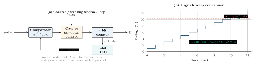
Counter ADC feedback and its input-dependent DAC ramp. A tracking variant retains the previous code and moves one LSB per clock toward the input.
Conversion time depends on input amplitude:
plus reset, acquisition and latch overhead. For uniformly distributed input codes, average search time is about clocks. The architecture is simple and low cost, but much slower than SAR because it performs a linear search instead of a binary search.
A tracking or servo ADC retains its previous code. An up/down counter increments when and decrements when . It follows slowly varying inputs quickly but moves only one LSB per clock, so a basic tracking condition is
Rapid input steps require many clocks and comparator chatter can make the code toggle around one transition.
Successive-Approximation (SAR) ADC
Section titled “Successive-Approximation (SAR) ADC”A successive-approximation-register ADC performs a binary search. It holds the input constant, tentatively sets one bit from MSB to LSB, converts that trial code back to analog, and retains or clears the bit according to one comparator decision. Conversion therefore has fixed duration independent of input value.
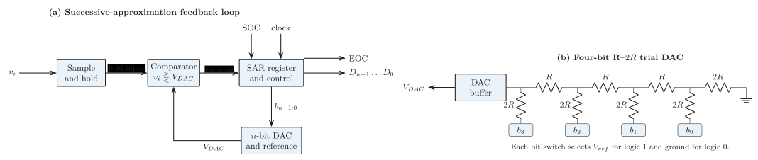
A SAR ADC uses comparator feedback to run a binary search; the trial code drives a DAC, represented here by a four-bit R– ladder.
For straight-binary conversion, the trial DAC voltage is
Modern SARs often use a binary-weighted capacitive array rather than R–, but the bit-test algorithm and ideal transfer are the same.
Conversion algorithm
Section titled “Conversion algorithm”-
Acquire and hold ; clear the register and assert start of conversion (SOC).
-
Tentatively set the MSB, giving .
-
If retain the bit; otherwise clear it.
-
Tentatively set the next bit while preserving earlier decisions. Repeat comparison through the LSB.
-
After decisions, latch the code and assert end of conversion (EOC).
The internal decision time is approximately
The held input must not move enough to alter a decision during those trials.
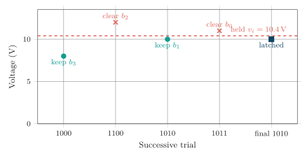
Four-bit SAR conversion: a retained bit moves the trial upward; a cleared bit moves it downward, halving the remaining search interval each time.
SAR offers an excellent speed, resolution, power and area compromise, commonly 8–18 bits. Its limits include S/H acquisition, reference settling, DAC matching/linearity, comparator offset/noise and clock feedthrough. Applications include microcontrollers, multiplexed sensor interfaces, data acquisition and digital instrumentation.
Pipeline and Two-Step ADCs
Section titled “Pipeline and Two-Step ADCs”Half-flash (two-step subranging) ADC
Section titled “Half-flash (two-step subranging) ADC”A half-flash ADC, also called a two-step or subranging ADC, divides an -bit conversion into a coarse Flash decision and a fine Flash decision. A DAC reconstructs the coarse result; the converter subtracts it from the same held input and quantizes the remaining residue to obtain the lower bits.
“Half-flash” means that the output bits are approximately divided between two Flash stages; it does not mean that the circuit uses exactly half as many comparators as a full Flash ADC. For an 8-bit design, a split is natural. The input must remain held while both decisions, the DAC reconstruction and the residue operation take place.
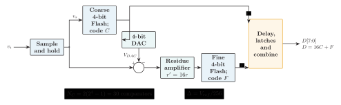
Ideal 8-bit half-flash (two-step subranging) ADC. The residue gain expands one coarse-code interval to the fine ADC’s full input range; without this block, the fine ADC must instead use a range of .
Main blocks and their roles
Section titled “Main blocks and their roles”The conversion path contains seven functional blocks:
| Block | Function |
|---|---|
| Sample-and-hold | Captures and keeps one value constant throughout both conversion steps. |
| Coarse 4-bit Flash | Locates the held input in one of 16 coarse ranges and produces the four MSBs . |
| -bit DAC | Reconstructs the lower boundary of the selected coarse range. |
| Subtractor | Forms the residue , the part not represented by the coarse code. |
| Residue amplifier | Usually multiplies by so one coarse interval occupies the fine Flash ADC’s full range. |
| Fine 4-bit Flash | Quantizes the scaled residue and produces the four LSBs . |
| Delay/latches and logic | Delays the early MSBs, aligns both results and forms the final 8-bit word; practical designs may also correct redundant decisions. |
Blocks in an 8-bit half-flash ADC.
General conversion law
Section titled “General conversion law”Let the coarse stage resolve bits and the fine stage resolve bits, so . For a unipolar input ,
The ideal coarse conversion, DAC reconstruction and residue are
where . A residue gain expands this interval to the fine ADC’s full range:
The aligned result is the concatenation
For an ideal converter, and . If the residue is not amplified, the fine ADC must instead have full-scale span ; its local step is then .
Step-by-step operation
Section titled “Step-by-step operation”-
Sample: the S/H acquires and enters hold mode.
-
Coarse conversion: the first 4-bit Flash ADC selects one of 16 coarse ranges and outputs , the four MSBs.
-
Reconstruction: the DAC converts to the analog coarse estimate .
-
Residue extraction: the subtractor forms ; ideally .
-
Fine conversion: either is amplified by and applied to a full-range 4-bit Flash ADC, or an unamplified residue is applied to a fine ADC whose range is .
-
Alignment: latches retain the earlier MSBs until the LSBs are ready, then logic forms .
Timing and practical errors
Section titled “Timing and practical errors”The decisions are sequential. A nonpipelined half-flash latency is approximately
where includes DAC, subtractor, residue-gain and settling time. Thus it is slower than a full Flash ADC but normally much faster than an -step iterative converter. It cannot automatically accept one new sample per clock; interstage holding and pipelining are required to overlap conversions.
Important error sources are coarse-comparator offset and bubbles, coarse-DAC INL, subtractor offset, residue-gain error/nonlinearity, incomplete settling, S/H droop, reference mismatch and fine-comparator offset/noise. In a strict concatenation, a wrong coarse decision near a subrange boundary can move the output by 16 final LSBs. Practical converters therefore often provide overlap or redundant bits: the fine stage covers beyond one nominal coarse interval, and digital correction combines overlapping stage decisions. This tolerates bounded coarse-comparator and residue errors, but it does not fix arbitrary gross errors or an unsettled residue.
Half-flash ADCs offer much lower input capacitance, area and comparator power than full Flash at the same nominal resolution. Their costs are extra latency, a precision DAC/residue path, interstage matching and calibration complexity. They are useful in video, imaging, communication receivers and high-speed instrumentation where full Flash is too large or power hungry but SAR speed is insufficient.
Pipeline ADC
Section titled “Pipeline ADC”A pipeline ADC divides conversion among clocked stages. Each stage samples its input residue, resolves a few coarse bits with a small sub-ADC, converts those bits back through a sub-DAC, subtracts that estimate and amplifies the remaining residue for the next stage.
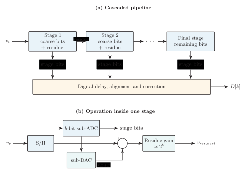
Pipeline ADC. Each stage resolves a few coarse bits, subtracts their DAC estimate, amplifies the residue and passes it to the next clocked stage.
For an ideal stage resolving bits,
Here is the integer gain exponent of a nonredundant ideal stage. The stage bits emerge on different clock cycles, so digital logic delays, aligns and combines them. A conventional “1.5-bit” stage has three decision regions, contributes roughly one effective bit and normally uses residue gain , not ; its redundant range permits correction of finite sub-comparator offset.
Once all stages are full, a pipeline can deliver one conversion per clock even though one sample needs several clocks to traverse the chain:
It therefore offers high throughput at medium/high resolution, but incurs multi-cycle latency, residue-amplifier settling and gain errors, sub-DAC linearity limits, clocking complexity and substantial analog power. Typical uses include video, intermediate-frequency digitization and high-speed data acquisition.
Single-Slope and Dual-Slope Integrating ADCs
Section titled “Single-Slope and Dual-Slope Integrating ADCs”An integrating ADC converts voltage into a measured time or count by using an op-amp integrator. A single-slope converter times one calibrated ramp; a dual-slope converter first integrates the unknown for a fixed time and then measures the time required by an opposite reference to return the integrator to zero.
Integrating conversion deliberately trades speed for averaging, high DC resolution and good rejection of periodic interference. It suits slowly varying measurements and instruments, especially digital multimeters, weighing systems and precision panel meters; it is generally unsuitable for high-bandwidth, continuous waveform acquisition.
Single-slope (ramp) ADC
Section titled “Single-slope (ramp) ADC”A single-slope ADC resets an integrator to zero, applies a constant reference of known polarity, and times the resulting linear ramp until it reaches the unknown input. In the figure, the applied input is , so an inverting integrator produces a positive ramp.
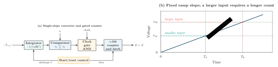
Single-slope ADC. A fixed-slope reference ramp is timed until it reaches the unknown input; the count changes if , , or the clock period changes.
With the capacitor initially discharged,
The comparator changes state when , hence
If the clock period is and the counter records approximately pulses,
A larger input therefore needs a longer ramp time and produces a larger count; the ramp slope itself remains fixed during one conversion.
Controller sequence
Section titled “Controller sequence”-
Momentarily close the reset switch to discharge the integrating capacitor and clear the counter.
-
Apply to the integrator and open the clock gate while .
-
Count clock pulses as the reference ramp rises linearly.
-
When reaches , the comparator closes the gate; latch the count as the output code.
-
Reset the integrator and counter before the next conversion.
The simplicity is attractive, but its scale depends directly on several analog and timing quantities. For fixed , small changes produce approximately
Resistor/capacitor tolerance and temperature coefficient, capacitor ageing and leakage, reset residue, integrator offset, comparator offset and clock error all change the result. Conversion time is also input-dependent and approaches near full scale when the ramp is calibrated for an -bit count. These limitations make the basic single-slope ADC unsuitable for precision measurement without frequent calibration.
Dual-slope ADC
Section titled “Dual-slope ADC”A dual-slope ADC removes the first-order dependence on , and clock period by using the same integrator and clock in two opposite-slope phases. It first integrates the unknown input for a fixed run-up interval , then applies a known opposite-polarity reference and counts the variable run-down interval required to return to zero.
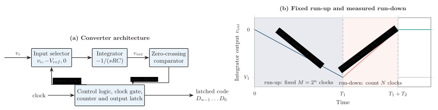
Dual-slope ADC architecture and counter-controlled sequence: a fixed -clock run-up followed by a measured -clock run-down.
Phase 0: reset or auto-zero
Section titled “Phase 0: reset or auto-zero”The capacitor and counter are reset. Practical converters may also measure and store integrator/comparator offset during an auto-zero interval. Residual charge must be small enough that each conversion begins from the same initial state.
Phase 1: fixed-time run-up
Section titled “Phase 1: fixed-time run-up”The switch applies for a prescribed clock periods, ; commonly . For a constant positive input,
The integrator ramps negative. A counter overflow or timing register marks the end of exactly clocks, changes the input switch to and clears or restarts the run-down counter.
Phase 2: measured run-down
Section titled “Phase 2: measured run-down”The opposite reference produces a positive slope. At time after run-down begins,
The zero-crossing comparator keeps the clock gate open until . Therefore
With and ,
For , the latched run-down count is ideally . The nominal unipolar range remains half-open, , so the largest valid -bit count is ; an exact or larger full-scale input must be treated as overrange.
Counter and switch sequence
Section titled “Counter and switch sequence”-
Reset/auto-zero the integrator and counter.
-
Select and integrate for exactly clocks. With an -bit timing counter, overflow after clocks can change the switch.
-
Select , restart the counter at zero and continue clocking while the integrator output has not crossed zero.
-
At the zero crossing, close the clock gate and latch the run-down count ; compute or directly interpret .
Conversion time and resolution trade-off
Section titled “Conversion time and resolution trade-off”Ignoring reset and auto-zero overhead,
For and ,
Each added bit approximately doubles the fixed run-up and worst-case conversion time at the same clock frequency. Increasing reduces conversion time only until integrator settling, comparator response, switching and counter limits dominate.
Averaging and mains-noise rejection
Section titled “Averaging and mains-noise rejection”For a time-varying input, run-up measures its average over :
Rectangular integration has normalized magnitude response
with zeros at for nonzero integer . Choosing rejects ideal interference; choosing rejects . A run-up contains five 50-Hz periods and six 60-Hz periods, so it ideally rejects both. This averaging explains the excellent mains-noise immunity of integrating meters, although noninteger-frequency interference and front-end saturation are not eliminated.
| Feature | Single slope | Dual slope |
|---|---|---|
| Measured interval | Reference ramp until it reaches | Reference run-down after fixed-time input integration |
| Ideal result | ||
| dependence | Direct scale error | Cancels to first order between phases |
| Clock dependence | Clock period sets scale | Common clock period cancels in |
| Noise rejection | Little inherent averaging | Strong averaging; selectable notches at |
| Conversion time | Input-dependent, up to about | , up to about |
| Typical use | Simple low-cost conversion | DMMs and precision low-rate measurement |
Single-slope versus dual-slope conversion.
Dual-slope conversion offers high resolution, excellent DC accuracy and strong periodic-noise rejection with modest analog hardware. Its limitations are low throughput, input-dependent latency, reference error, integrator leakage and finite gain, dielectric absorption, comparator offset, switching charge and auto-zero overhead. It is preferred for slowly changing signals where measurement reliability matters more than acquisition speed.
Sigma-Delta () ADC
Section titled “Sigma-Delta (ΔΣ\Delta\SigmaΔΣ) ADC”A sigma-delta converter trades bandwidth for resolution. A high-rate feedback modulator produces a low-resolution, usually one-bit stream; a digital low-pass filter removes out-of-band quantization noise and a decimator reduces the rate to high-resolution output words.
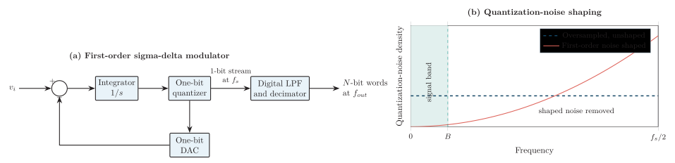
A first-order sigma-delta ADC produces a high-rate one-bit stream, shapes quantization noise out of band, then filters and decimates the result.
For signal bandwidth and modulator rate , the oversampling ratio is
The summer subtracts one-bit DAC feedback, the integrator accumulates this error (sigma operation), and the quantizer emits a pulse density representing input amplitude. A one-bit DAC is inherently monotonic because it has only two reference levels.
Oversampling spreads approximately fixed quantization-noise power across the wider Nyquist band; digital filtering retains only the small in-band fraction. Oversampling alone gains about SNR whenever OSR doubles. A linearized first-order modulator has approximately
so its noise-transfer function has a zero at DC. Quantization noise is suppressed in band and pushed to high frequency; a first-order loop ideally gains about in-band SNR per doubling of OSR. More generally, for ideal order ,
per doubling of OSR. The digital filter then rejects the shaped out-of-band noise and decimates to the required output rate.
Sigma-delta ADCs provide excellent linearity, noise rejection and 16–24-bit resolution with simple analog circuitry. Their limitations are restricted signal bandwidth, filter latency, clock-jitter sensitivity, digital complexity, idle tones and higher-order loop-stability concerns. They dominate audio, precision sensor and biomedical conversion.
Practical ADC Interface, Error Budget and Calibration
Section titled “Practical ADC Interface, Error Budget and Calibration”An ADC never operates in isolation. The signal source, anti-alias filter, driver, sampling network, reference, clock, supplies, printed-circuit layout and digital interface all contribute error or limit speed.
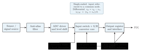
Practical ADC signal chain. Conversion accuracy depends on the source, driver, reference, clock, supplies, return paths and digital interface—not only on the nominal converter core.
Input range, polarity and common mode
Section titled “Input range, polarity and common mode”A single-ended ADC measures one input relative to a common reference. A differential ADC measures
Both pins must remain inside their specified common-mode range even when is valid. Differential drive rejects common coupled noise and even-order distortion, but does not remove reference, mismatch or clock errors. Unipolar, bipolar, pseudo-differential and fully differential ranges must therefore be distinguished before assigning codes.
Driver, reference, clock and layout
Section titled “Driver, reference, clock and layout”-
Input driver: Must charge the switched input capacitance within , absorb kickback, remain stable with the ADC load and preserve the required bandwidth and distortion.
-
Anti-alias network: Sets the wanted passband and attenuates all unwanted energy that would fold below . Its resistance and the ADC input capacitance also affect settling.
-
Reference: Sets every transition voltage. Check absolute accuracy, noise density, temperature coefficient, output impedance, load-transient recovery and local bypassing.
-
Clock: Its rms jitter limits high-frequency SNR; keep clock edges from coupling into the analog input and reference.
-
Supplies and layout: Keep analog/reference loops short, provide local decoupling, control return-current paths and prevent digital output currents from sharing sensitive analog impedance.
Reference variation is a scale error. For a fixed output code interpreted as an analog estimate in a unipolar converter, a small reference change produces approximately
Input-referred white noise density integrated over effective noise bandwidth gives the useful estimate
Error budgeting and calibration
Section titled “Error budgeting and calibration”For error contributions expressed in the same units at one operating point, a conservative worst-case bound and an independent-error estimate are
Use worst-case addition when guaranteed limits must hold simultaneously; use root-sum-square only for sufficiently independent random terms. A two-point calibration can remove much of offset and gain error, but it cannot remove quantization, random noise, missing codes or detailed INL shape. Calibration conditions must remain representative of reference, temperature and loading.
Architecture Comparison and Selection
Section titled “Architecture Comparison and Selection”| Type | Decision method | Timing behavior | Representative bits | Best fit and principal limitations |
|---|---|---|---|---|
| Flash | All thresholds in parallel | Comparator + encoder delay; highest raw speed | –10 | Scopes, radar, direct IF; exponential power, area, input capacitance and matching. |
| Half-flash | Coarse Flash, DAC/residue path, then fine Flash | Two sequential decisions plus residue settling | –12 | Video and fast DAQ; far fewer comparators than Flash, but residue accuracy limits. |
| Counter / tracking | DAC feedback with linear up/down search | Input dependent; worst counter case clocks | –12 | Simple controls and slowly varying signals; poor step response and low speed. |
| SAR | DAC feedback with MSB-to-LSB binary search | Fixed decisions plus acquisition | –20 | General DAQ and MCUs; DAC/reference settling and acquisition limit accuracy/speed. |
| Pipeline | Coarse sub-ADC, sub-DAC subtraction and residue gain per stage | One output/clock after fill; multi-cycle latency | –16 | Video and IF; residue gain/settling, calibration, clocking and analog power. |
| Single-slope | Fixed reference ramp timed to the input crossing | Input-dependent; up to about clocks | –12 | Simple low-cost conversion; , ramp, comparator and clock drift limit accuracy. |
| Dual-slope | Fixed run-up, timed reference run-down | ; very slow but deterministic ratio | –22 | DMMs/precision DC; strong mains rejection, leakage and reference drift. |
| Sigma-delta | Oversampled feedback, noise shaping and digital decimation | Many modulator clocks plus filter latency | –24 | Audio/precision sensors; limited signal bandwidth, latency, idle tones and loop limits. |
Practical comparison of the principal ADC architectures.
The bit ranges are representative, not hard physical boundaries. Process, calibration, bandwidth and power targets can move them substantially.
Scaling check: At , Flash needs comparators, two 6-bit Flash stages need only comparators before redundancy and correction hardware, a counter ADC can need trial clocks, SAR needs , and a filled pipeline can output one word per clock after its latency, and a dual-slope converter with can need nearly clocks. The tabulated bit ranges are representative, not hard architectural limits.
Reference Definitions and Architecture Mechanisms
Section titled “Reference Definitions and Architecture Mechanisms”Core definitions
Section titled “Core definitions”| Term | Definition |
|---|---|
| ADC | Circuit that samples an analog input, quantizes each held sample to one of finite levels and encodes the selected level as a digital word. |
| Bit depth | Number of bits in one output word; it provides possible codes. |
| Resolution | Smallest ideal code interval: , also stated as bits or of span. |
| Reference voltage | Precision analog standard that establishes the ADC transfer scale and its ideal transition voltages. |
| Sampling rate | Number of sampling instants per second, ; its associated Nyquist frequency is . |
| Quantization | Irreversible assignment of a continuous-amplitude sample to one finite code bin. |
| Quantization error | Difference between the actual sample and represented level; ideally $ |
| Single-slope | Integrating ADC that counts the time for a fixed reference ramp to reach the unknown input; its scale depends on . |
| Dual-slope | Integrating ADC that applies the input for a fixed time, then counts an opposite-reference return to zero; cancels ideally. |
| Half-flash | Two-step ADC that resolves coarse bits, subtracts their DAC value and quantizes the remaining residue for the fine bits. |
| Conversion time | Internal time needed to determine one result after conversion begins. |
| Latency | Time from sampling instant to availability of that sample’s valid output code. |
| Throughput | Number of completed output codes per second after any pipeline is full. |
| DNL / INL | Code-width error relative to 1 LSB / transition deviation from a specified ideal straight line. |
| ENOB | Number of ideal bits giving the measured SINAD: . |
Core ADC definitions.
| Architecture | Core mechanism |
|---|---|
| Flash | Parallel comparators test every threshold simultaneously, minimizing latency but requiring exponentially more hardware. |
| Half-flash | A coarse Flash/DAC stage forms a residue that a second Flash stage resolves, reducing comparators at the cost of residue settling. |
| Counter | A DAC code rises one LSB per clock until it crosses the input, so time depends on input and can approach clocks. |
| SAR | A feedback DAC performs an MSB-to-LSB binary search, giving a fixed comparator decisions. |
| Pipeline | Clocked stages resolve coarse bits and amplify residue, giving one output per clock after multi-cycle latency. |
| Single-slope | A fixed reference ramp is timed until it reaches the input; simple hardware leaves the result sensitive to ramp and clock scale. |
| Dual-slope | Fixed-time integration of the input followed by timed opposite-reference integration gives an accurate ratio and rejects periodic noise. |
| Sigma-delta | Oversampling and feedback shape quantization noise out of band; digital filtering and decimation recover high in-band resolution. |
ADC architecture mechanism summary.