Flip-Flops
SR Latch
Section titled “SR Latch”Definition / Introduction
Section titled “Definition / Introduction”An SR (Set–Reset) latch is the most basic bistable memory element in sequential logic. It is built from two cross-coupled NOR gates (active-HIGH inputs) or two cross-coupled NAND gates (active-LOW inputs). Being level-sensitive, it has no clock, stores a single bit, and has two inputs S (Set) and R (Reset) with two complementary outputs Q and .
Logic Symbol
Section titled “Logic Symbol”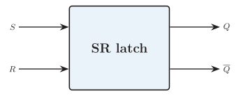
SR latch logic symbol
Circuit Diagram / Internal Operation
Section titled “Circuit Diagram / Internal Operation”NOR implementation (active-HIGH inputs):
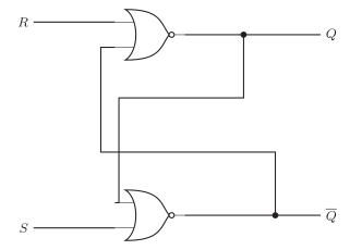
Cross-coupled NOR SR latch
NAND implementation (active-LOW inputs ):
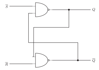
Cross-coupled NAND SR latch
Truth Table
Section titled “Truth Table”| Operation | |||
|---|---|---|---|
| 0 | Hold (no change) | ||
| 0 | 1 | 0 | Reset |
| 1 | 0 | 1 | Set |
| 1 | 1 | Invalid | Forbidden |
Working / Operation
Section titled “Working / Operation”-
S = 0, R = 0 — Hold: the latch retains its previous state, .
-
S = 0, R = 1 — Reset: the output is forced to .
-
S = 1, R = 0 — Set: the output is forced to .
-
S = 1, R = 1 — Forbidden: both outputs go LOW, so and are no longer complementary.
Timing Diagram
Section titled “Timing Diagram”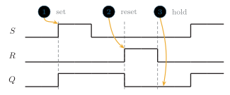
SR latch timing diagram: an S pulse sets Q, an R pulse resets it, and it holds between pulses
Characteristic Equation & Excitation Table
Section titled “Characteristic Equation & Excitation Table”Excitation table:
| 0 | 0 | ||
| 0 | 1 | 1 | 0 |
| 1 | 0 | 0 | 1 |
| 1 | 1 | 0 |
Forbidden (Invalid) State
Section titled “Forbidden (Invalid) State”For the NOR latch, S = R = 1 drives both outputs LOW, violating the complementary condition. If both inputs then return to 0 simultaneously, the final state depends on unequal gate delays (a race), so the result is unpredictable. The equivalent NAND latch uses active-LOW inputs and its forbidden condition is .
Applications
Section titled “Applications”-
Switch debouncing circuits
-
Basic 1-bit memory / set–reset control
-
Building block of all clocked flip-flops
-
Simple asynchronous storage element
SR Flip-Flop
Section titled “SR Flip-Flop”Definition / Introduction
Section titled “Definition / Introduction”An SR flip-flop is a clocked (synchronous) version of the SR latch. It has inputs S and R, a clock input CLK, and complementary outputs Q and . In the positive-edge form used here, the S and R inputs are sampled only at the rising edge of CLK, so the state does not follow them continuously.
The symbol and timing example in this subsection use positive-edge triggering. The steering-gate circuits below are the underlying CLK-HIGH level-gated SR latch forms; an edge-triggered device adds internal clock-edge isolation around this storage function.
Logic Symbol
Section titled “Logic Symbol”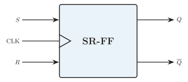
Clocked SR flip-flop symbol
Level-Gated Building Blocks / Internal Operation
Section titled “Level-Gated Building Blocks / Internal Operation”AND-gate steering (active-HIGH SR latch):
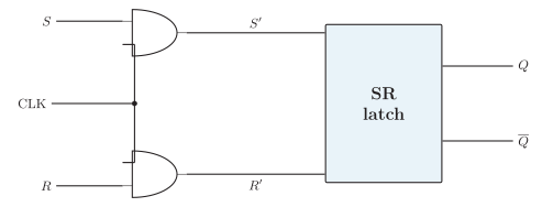
Gated SR flip-flop with AND steering into an active-HIGH SR latch
NAND-gate steering (active-LOW SR latch):
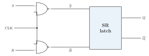
Gated SR flip-flop with NAND steering into an active-LOW SR latch
Truth Table (at )
Section titled “Truth Table (at CLK↑\mathrm{CLK}\uparrowCLK↑)”| Operation | |||
|---|---|---|---|
| 0 | Hold | ||
| 0 | 1 | 0 | Reset |
| 1 | 0 | 1 | Set |
| 1 | 1 | Invalid | Forbidden |
Between rising clock edges, the output holds for any , .
Working / Operation
Section titled “Working / Operation”-
S = 0, R = 0: no change, .
-
S = 0, R = 1: reset, .
-
S = 1, R = 0: set, .
-
S = 1, R = 1: forbidden, output is indeterminate.
Timing Diagram
Section titled “Timing Diagram”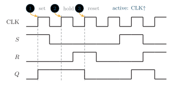
Positive-edge SR flip-flop timing diagram: successive rising edges set, hold, and reset Q
Characteristic Equation & Excitation Table
Section titled “Characteristic Equation & Excitation Table”Excitation table:
| 0 | 0 | ||
| 0 | 1 | 1 | 0 |
| 1 | 0 | 0 | 1 |
| 1 | 1 | 0 |
Limitation (Invalid State)
Section titled “Limitation (Invalid State)”The SR flip-flop still has the forbidden input S = R = 1, which makes the next state undefined. This drawback is removed by the JK flip-flop, where is redefined as a toggle instead of an invalid command.
Applications
Section titled “Applications”-
Synchronous set/reset control
-
Basic clocked memory cell
-
Building block for D, JK, and T flip-flops
-
Timing-controlled storage in synchronous systems
D Latch
Section titled “D Latch”Definition / Introduction
Section titled “Definition / Introduction”A D (Data or Delay) latch is a level-sensitive storage element with a single data input D and an enable (EN) input. It is obtained from an SR latch by connecting and , which removes the forbidden state. While enabled it is transparent (output follows ); when disabled it holds the last value.
Logic Symbol
Section titled “Logic Symbol”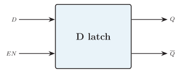
D latch symbol
Circuit Diagram / Internal Operation
Section titled “Circuit Diagram / Internal Operation”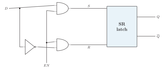
D latch built from an SR latch
Truth Table
Section titled “Truth Table”| Operation | |||
|---|---|---|---|
| Hold (latched) | |||
| 1 | 0 | 0 | Store 0 (transparent) |
| 1 | 1 | 1 | Store 1 (transparent) |
( = don’t-care)
Working / Operation
Section titled “Working / Operation”-
EN = 0: the input is blocked and the latch keeps its stored value.
-
EN = 1, D = 0: output becomes .
-
EN = 1, D = 1: output becomes .
Timing Diagram
Section titled “Timing Diagram”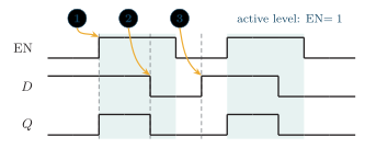
D latch timing diagram: Q follows D while EN is high and holds when EN is low
Characteristic Equation & Excitation Table
Section titled “Characteristic Equation & Excitation Table”Excitation equation:
Excitation table:
| 0 | 0 | |
| 0 | 1 | 1 |
| 1 | 0 | 0 |
| 1 | 1 | 1 |
Special Feature — Transparency
Section titled “Special Feature — Transparency”While EN = 1, the D latch is transparent: any change in passes straight to . This continuous following is undesirable in synchronous systems, so an edge-triggered D flip-flop is used when the data must be captured at a single instant.
Applications
Section titled “Applications”-
Temporary data latching on a bus
-
Register storage in latch-based designs
-
Holding a data value while other logic settles
-
Building block of the master–slave D flip-flop
D Flip-Flop
Section titled “D Flip-Flop”Definition / Introduction
Section titled “Definition / Introduction”A D (Data) flip-flop is an edge-triggered storage element with a single data input D, a clock input CLK, and complementary outputs Q and . It samples only at the active clock edge and copies it to the output after the clock-to- propagation delay. It has no invalid state.
Logic Symbol
Section titled “Logic Symbol”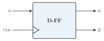
D flip-flop symbol
Circuit Diagram / Internal Operation (master–slave)
Section titled “Circuit Diagram / Internal Operation (master–slave)”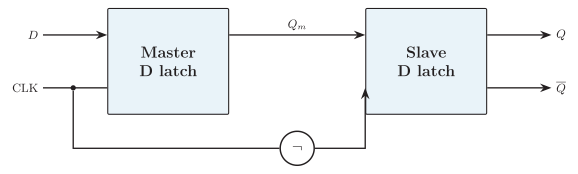
Master–slave D flip-flop
Truth Table (at )
Section titled “Truth Table (at CLK↑\text{CLK}\uparrowCLK↑)”| Operation | ||
|---|---|---|
| 0 | Reset / store 0 | |
| 1 | 1 | Set / store 1 |
Working / Operation
Section titled “Working / Operation”-
D = 0: at the active edge the output becomes .
-
D = 1: at the active edge the output becomes .
-
Between edges the output is held regardless of .
Timing Diagram
Section titled “Timing Diagram”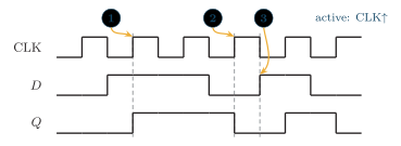
D flip-flop timing diagram: Q samples D on each rising clock edge
Characteristic Equation & Excitation Table
Section titled “Characteristic Equation & Excitation Table”Excitation equation:
Excitation table:
| 0 | 0 | |
| 0 | 1 | 1 |
| 1 | 0 | 0 |
| 1 | 1 | 1 |
Setup and Hold Time
Section titled “Setup and Hold Time”For reliable capture, must be stable for the setup time before the edge and the hold time after the edge. Violating either can drive the device into metastability, where the output takes an unpredictable time to settle. An asynchronous input should pass through a synchronizer before entering synchronous logic.
Applications
Section titled “Applications”-
Registers and shift registers
-
Data synchronizers for asynchronous inputs
-
Frequency division (with fed back to )
-
Pipeline stages and finite-state machines
JK Flip-Flop
Section titled “JK Flip-Flop”Definition / Introduction
Section titled “Definition / Introduction”The JK flip-flop is an improved version of the SR flip-flop. It has two data inputs J and K, a clock input CLK, and two complementary outputs Q and . Unlike the SR flip-flop, the condition J = K = 1 is valid and causes the output to toggle, removing the invalid-state problem.
The symbol and timing example use a positive-edge-triggered JK flip-flop. The NAND network below is its CLK-HIGH level-gated precursor; it exposes the feedback path responsible for race-around when the clock pulse is too wide.
Logic Symbol
Section titled “Logic Symbol”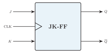
JK flip-flop symbol
Level-Gated NAND Precursor / Internal Operation
Section titled “Level-Gated NAND Precursor / Internal Operation”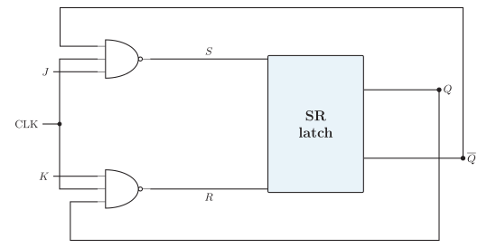
JK flip-flop from NAND gates and an SR latch
Truth Table (at )
Section titled “Truth Table (at CLK↑\text{CLK}\uparrowCLK↑)”| Operation | |||
|---|---|---|---|
| 0 | Hold | ||
| 0 | 1 | 0 | Reset |
| 1 | 0 | 1 | Set |
| 1 | 1 | Toggle |
The characteristic feature is that J = K = 1 produces toggling, eliminating the invalid state of the SR flip-flop.
Working / Operation
Section titled “Working / Operation”-
J = 0, K = 0 — Hold: ; the flip-flop retains its state.
-
J = 0, K = 1 — Reset: regardless of the present state.
-
J = 1, K = 0 — Set: regardless of the present state.
-
J = 1, K = 1 — Toggle: ; the output changes on every active clock event.
Timing Diagram
Section titled “Timing Diagram”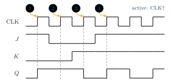
JK flip-flop timing diagram: set, hold, reset, and toggle at successive clock edges
Characteristic Equation & Excitation Table
Section titled “Characteristic Equation & Excitation Table”Excitation table:
| 0 | 0 | ||
| 0 | 1 | 1 | |
| 1 | 0 | 1 | |
| 1 | 1 | 0 |
Race-Around Condition
Section titled “Race-Around Condition”In a level-triggered JK flip-flop, when J = K = 1 and the clock stays HIGH longer than the propagation delay, the output can toggle many times in one clock pulse:
This unstable behavior is the race-around condition. Prevention:
-
Use an edge-triggered JK flip-flop (responds only at one clock edge).
-
Use a master–slave JK flip-flop, so only one transition occurs per clock cycle.
Applications
Section titled “Applications”-
Counters (ripple and synchronous)
-
Frequency dividers (toggle mode divides frequency by 2)
-
Shift registers and sequence generators
-
General sequential-control circuits
Master–Slave JK Flip-Flop
Section titled “Master–Slave JK Flip-Flop”Definition / Introduction
Section titled “Definition / Introduction”The master–slave JK flip-flop is a cascade of two JK latches — a master and a slave — driven by complementary clocks. It is designed to eliminate the race-around condition by allowing the external output to change only once per clock cycle.
For the phase assignment drawn here, the master is open at CLK = 1 and the slave at CLK = 0, so the external output changes on the falling clock edge.
Logic Symbol
Section titled “Logic Symbol”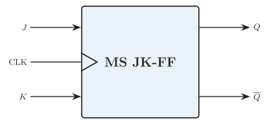
Master–slave JK flip-flop symbol
Circuit Diagram / Internal Operation
Section titled “Circuit Diagram / Internal Operation”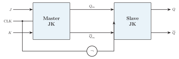
Master–slave JK flip-flop
Truth Table (at )
Section titled “Truth Table (at CLK↓\text{CLK}\downarrowCLK↓)”| Operation | |||
|---|---|---|---|
| 0 | Hold | ||
| 0 | 1 | 0 | Reset |
| 1 | 0 | 1 | Set |
| 1 | 1 | Toggle |
Working / Operation
Section titled “Working / Operation”-
The master samples and during the active clock level.
-
The slave transfers the master state to the output at the end of that level.
-
Because the master is isolated from the output while the slave updates, feedback cannot cause repeated toggling.
Timing Diagram
Section titled “Timing Diagram”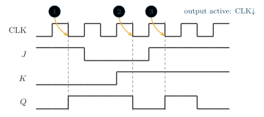
Falling-edge master-slave JK timing diagram: the output updates once per clock cycle
Characteristic Equation & Excitation Table
Section titled “Characteristic Equation & Excitation Table”Excitation table:
| 0 | 0 | ||
| 0 | 1 | 1 | |
| 1 | 0 | 1 | |
| 1 | 1 | 0 |
Elimination of Race-Around
Section titled “Elimination of Race-Around”Since the master and slave are never transparent at the same time, the output can change at most once per clock cycle, even when . This removes the race-around condition of the level-triggered JK flip-flop. (A residual limitation is ones/zeros catching, solved by a true edge-triggered design.)
Applications
Section titled “Applications”-
Reliable counters with many stages
-
Frequency dividers
-
Registers where race-around must be avoided
-
High-integrity sequential control
T Flip-Flop
Section titled “T Flip-Flop”Definition / Introduction
Section titled “Definition / Introduction”A T (Toggle) flip-flop is a single-input clocked flip-flop obtained from a JK flip-flop by tying (or from a D flip-flop with ). In the positive-edge form shown here, T = 1 toggles the output on each rising edge of CLK, while T = 0 holds it. It is the natural element for binary counting.
Logic Symbol
Section titled “Logic Symbol”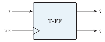
T flip-flop symbol
Circuit Diagram / Internal Operation
Section titled “Circuit Diagram / Internal Operation”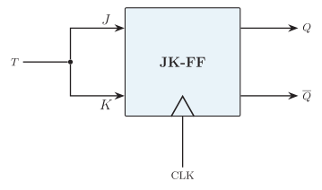
T flip-flop from a JK flip-flop
Truth Table (at )
Section titled “Truth Table (at CLK↑\text{CLK}\uparrowCLK↑)”| Operation | ||
|---|---|---|
| Hold | ||
| 1 | Toggle |
Working / Operation
Section titled “Working / Operation”-
T = 0 — Hold: ; the state is unchanged.
-
T = 1 — Toggle: ; the output inverts on every active clock edge.
Timing Diagram
Section titled “Timing Diagram”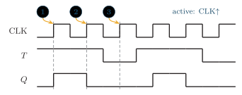
T flip-flop timing diagram: Q toggles when T is 1 and holds when T is 0
Characteristic Equation & Excitation Table
Section titled “Characteristic Equation & Excitation Table”Excitation equation:
Excitation table:
| 0 | 0 | |
| 0 | 1 | 1 |
| 1 | 0 | 1 |
| 1 | 1 | 0 |
Special Feature — Frequency Division
Section titled “Special Feature — Frequency Division”When T is held at 1, the output toggles once per clock edge, so its frequency is half the clock frequency:
Cascading such stages divides the clock by , which is the basis of ripple (asynchronous) counters.
Applications
Section titled “Applications”-
Binary and ripple counters
-
Frequency dividers ( per stage)
-
Toggle/control stages in synchronous counters
-
Simple on/off state control