Transmission Lines and Impedance Matching
Distributed Line Model
Section titled “Distributed Line Model”The primary line parameters are
| Symbol | Meaning | SI unit |
|---|---|---|
| series resistance per unit length | ||
| series inductance per unit length | ||
| shunt conductance per unit length | ||
| shunt capacitance per unit length |
Time-Domain Form
Section titled “Time-Domain Form”For instantaneous line voltage and current ,
Phasor Form
Section titled “Phasor Form”For sinusoidal steady state, , where and . The voltage and current phasors and therefore satisfy
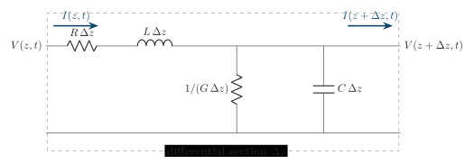
Distributed model of a uniform transmission line.
Propagation Constant and Characteristic Impedance
Section titled “Propagation Constant and Characteristic Impedance”It is
It is
For a lossless line,
Travelling Waves
Section titled “Travelling Waves”Thus,
Load Reflection
Section titled “Load Reflection”At the load,
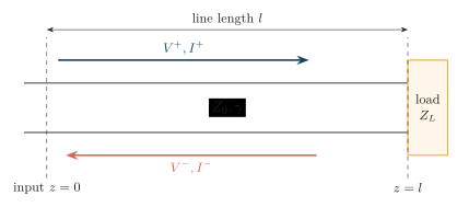
Reference directions for a line terminated in a load.
Special cases:
| Load | Reflection coefficient |
|---|---|
| Matched load, | |
| Open circuit | |
| Short circuit |
Standing Waves, VSWR and Return Loss
Section titled “Standing Waves, VSWR and Return Loss”Standing Waves
Section titled “Standing Waves”A load mismatch produces the reflected wave. Its interference with the incident wave creates fixed voltage maxima and minima along the line. Maxima are called antinodes; a minimum that reaches zero is called a node.
For load reflection coefficient ,
A matched load has and . As the mismatch increases, VSWR increases; complete reflection gives and .
Return Loss
Section titled “Return Loss”An ideal match has and . Complete reflection has and .
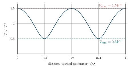
Voltage standing-wave envelope on a mismatched line.
Comparison
Section titled “Comparison”| Quantity | Meaning | Ideal match | Complete reflection |
|---|---|---|---|
| Standing-wave envelope | Voltage variation | Flat | Maximum |
| Voltage reflection magnitude | |||
| VSWR | |||
| Return loss (dB) | Logarithmic power ratio |
Input Impedance
Section titled “Input Impedance”For a lossless line of length , the terminal voltage and current are related to the load quantities by
Substituting , taking , and dividing numerator and denominator by gives the input-impedance transformation below.
For a lossless line of length terminated by ,
Important special lengths:
| Length | Input impedance |
|---|---|
Impedance Matching
Section titled “Impedance Matching”Quarter-Wave Transformer
Section titled “Quarter-Wave Transformer”-
Insert a section of characteristic impedance between the main line and a real load .
-
At the design frequency , make its electrical length , or , where is the wavelength in the transformer.
-
The match is exact at but is generally narrowband. A complex load must first be transformed to a real resistance for this simple formula to apply.
For a quarter-wave transformer matching a real load to a line ,
This condition follows directly from the input impedance of the transformer section:
At , , so the tangent terms dominate and
Requiring the main line to see gives . The quarter-wave section is therefore an impedance inverter at its design frequency.
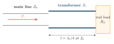
Quarter-wave transformer matching section.
L-Network Matching
Section titled “L-Network Matching”-
Ideal inductors and capacitors store energy without dissipating average power, so the network can provide a lossless conjugate match.
-
The series and shunt arrangement depends on which side has the higher resistance; the shunt element is placed on the high-resistance side in the topology shown below.
-
A series inductor with a shunt capacitor gives a low-pass match. Interchanging them gives the dual high-pass form.
-
L-networks are simple and useful when lumped components remain practical, but their match is frequency-sensitive.
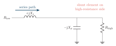
Low-pass L-match topology.
Single-Stub Matching
Section titled “Single-Stub Matching”-
For the shunt-stub arrangement shown, choose a distance from the load at which the normalized admittance is .
-
Choose the stub length so that it supplies susceptance ; the total normalized admittance then becomes , producing a match.
-
Open and shorted stubs are both possible. Stub matching is convenient at radio and microwave frequencies, where distributed lines replace lumped reactances.
-
The possible solutions repeat every and are generally narrowband.
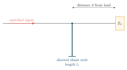
Single shunt-stub matching schematic.
Double-Stub Matching
Section titled “Double-Stub Matching”-
Only the two stub lengths need adjustment, so the method is useful when a single stub cannot be placed at its calculated distance from the load.
-
The first stub moves the admittance to a value that the second stub can transform to the chart centre.
-
Certain loads cannot be matched for some fixed stub spacings; these form a forbidden region. Double-stub matches are also frequency-sensitive.
Smith-Chart Design
Section titled “Smith-Chart Design”-
Normalize the load as ; for a shunt-stub design, convert it to admittance .
-
Move clockwise toward the generator on the constant- circle until the conductance circle is reached. The outer scale gives the distance from the load.
-
Move along the circle by adding the stub susceptance until the chart centre, , is reached. The corresponding scale reading gives .
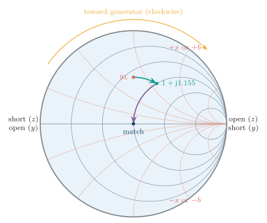
Smith chart path for shunt-stub matching.
Matching Method Comparison
Section titled “Matching Method Comparison”| Feature | Quarter-wave transformer | Single stub | Double stub |
|---|---|---|---|
| Elements | one line section | one open or short stub | two fixed-position stubs |
| Direct load | real in its basic form | real or complex | real or complex, with forbidden regions |
| Adjustment | section impedance and length | stub length and position | two stub lengths |
| Installation | needs a different line impedance | needs access at a calculated point | useful when connection points are fixed |
| Bandwidth | narrowband | narrowband | narrowband |
All three methods make the impedance seen by the main line equal to at the design frequency. The choice is governed mainly by load type, available line impedances, accessible connection points and tuning needs.
Worked Example
Section titled “Worked Example”A line is terminated by a real load. The load reflection coefficient is
Therefore
The reflected power fraction is , or about . To match the same load with a quarter-wave section,
At the design frequency, this section presents to the main line, eliminating the reflection there.