Bipolar Transistor Switching Characteristics
A bipolar junction transistor (BJT) is a current-controlled, three-terminal device. In a switching circuit it is deliberately driven between cutoff (OFF, approximately an open circuit) and saturation (ON, approximately a closed switch). The forward-active region is useful for amplification, but in a switch it is crossed only during a transition.
Static Switching States
Section titled “Static Switching States”For the grounded-emitter NPN circuit in the figure, a HIGH input supplies base current and produces a LOW collector output. The stage is therefore both a switch and a logical inverter.
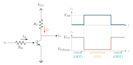
Grounded-emitter BJT switch and its inverted collector-output waveform.
| Region | Junction bias | Useful relation | Switch interpretation |
|---|---|---|---|
| Cutoff | B–E is not forward biased; B–C is reverse biased | , , | OFF; open switch |
| Forward active | B–E forward biased; B–C reverse biased | while the load permits it | Transition/amplifier region |
| Saturation | B–E and B–C both forward biased | , commonly – | ON; closed switch with a small voltage drop |
Bias conditions and terminal quantities in the three BJT regions.
DC Load Line and Saturation Design
Section titled “DC Load Line and Saturation Design”Applying KVL around the collector circuit gives
Thus the DC load line joins the two intercepts and . Increasing base drive moves the operating point from cutoff toward saturation, as shown in the figure.
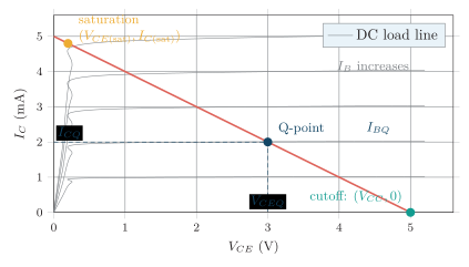
Representative BJT output characteristics and DC load line for and .
At the ON endpoint the load, not the transistor’s active-region gain, fixes the collector current:
Because transistor gain varies widely with device, current and temperature, a designer chooses a conservative forced beta , normally smaller than the guaranteed . Equivalently, an overdrive factor (ODF) may be specified:
Dynamic Switching Characteristics
Section titled “Dynamic Switching Characteristics”Switching is not instantaneous. Junction capacitances must be charged during turn-on, and excess minority-carrier charge accumulated in saturation must be removed during turn-off. The standard definitions use the 10% and 90% levels of the final collector current.
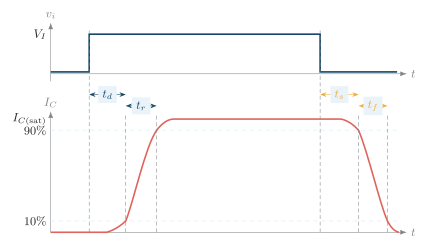
Input pulse and collector-current response showing the standard BJT switching-time construction. Since , the collector voltage waveform is inverted.
| Interval | Measurement definition | Main physical event |
|---|---|---|
| Delay | Input transition to | Charging the B–E depletion/diffusion capacitances to establish conduction |
| Rise | rises from 10% to 90% | Transit through the active region toward saturation |
| Storage | Input is removed or reversed until first falls to 90% | Removal/recombination of excess base charge stored in saturation |
| Fall | falls from 90% to 10% | Junction capacitances discharge and the transistor returns to cutoff |
Definitions and physical origins of BJT switching times.
Stored Charge and Speed Improvement
Section titled “Stored Charge and Speed Improvement”When the transistor is overdriven, both junctions are forward biased and the base contains excess minority carriers. If the excess stored charge at the start of turn-off is and a nearly constant reverse base current removes it, the useful first-order design estimate is
The exact logarithmic charge-control expression depends on the forward and reverse drive network; therefore or should not be treated as universal identities. The robust conclusions are that deeper saturation increases , while stronger reverse drive removes it faster.
| Method | Action | Trade-off or use |
|---|---|---|
| Schottky/Baker clamp | Clamps the B–C junction before it becomes strongly forward biased, preventing deep saturation | Greatly reduces ; used in Schottky TTL |
| Reverse base drive | Applies negative base current at turn-off to sweep out stored carriers | Fast turn-off, but the driver must tolerate bidirectional base current |
| Speed-up capacitor | Places a small capacitor across to deliver brief turn-on and turn-off current pulses | Reduces edge delay; must limit peak base current and ringing |
| Controlled overdrive | Uses only enough base current for guaranteed saturation | Balances low against storage delay |
| Reduced carrier lifetime | Process treatment reduces recombination lifetime | Improves speed at the cost of increased leakage |
Methods for reducing BJT switching time.