Power Electronics: Thyristor-Controlled Rectifiers
This section develops the SCR structure, two-transistor equivalent and – characteristic, derives controlled-rectifier average voltage, and compares switched-mode and linear supplies. Rectifier formulas depend on the load and on whether load current is continuous or discontinuous; those conditions are stated with each result.
Silicon-Controlled Rectifier (SCR)
Section titled “Silicon-Controlled Rectifier (SCR)”A silicon-controlled rectifier is a unidirectional, four-layer , three-junction power device with anode (A), cathode (K) and gate (G) terminals. It is a bistable, latching switch: a gate pulse can turn it on while it is forward biased, but the gate cannot normally turn it off.
The anode is connected to the outer layer, the cathode to , and the gate to the inner layer near the cathode. The central junction is the forward-blocking junction.
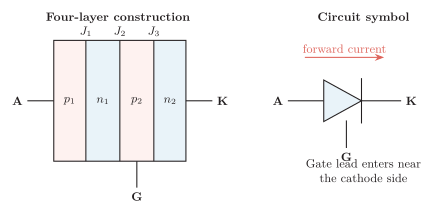
Native representation of SCR --- construction and symbol.
Operating states
Section titled “Operating states”-
Reverse blocking: A is negative with respect to K. Junctions and are reverse biased and only reverse leakage flows. Reverse breakdown is normally destructive.
-
Forward blocking: A is positive and . Junctions are forward biased, but is reverse biased. The device blocks until the forward breakover voltage is reached.
-
Forward conduction: A positive gate-current pulse injects carriers into and starts regeneration. The SCR snaps to a low on-state voltage, typically about –, and anode current is then limited by the external circuit.
Two-transistor regeneration
Section titled “Two-transistor regeneration”The four layers can be separated into a PNP transistor and an NPN transistor . Each collector supplies the other transistor’s base current, creating positive feedback. The gate injects current into the base region of .
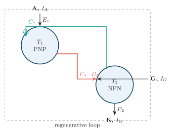
Cross-coupled PNP–NPN equivalent of an SCR.
Let be the common-base current gains and the collector leakage currents. Then
Kirchhoff’s current law gives and . Therefore
– characteristic
Section titled “VVV–III characteristic”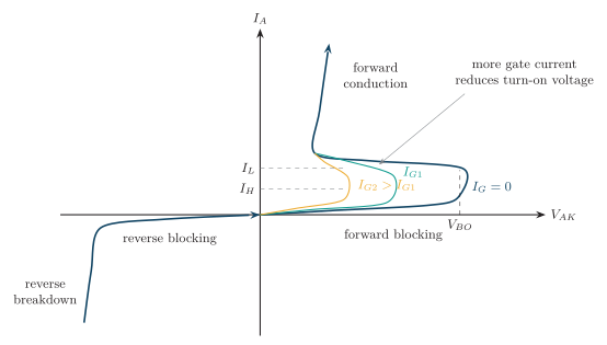
SCR static characteristic; the gate shifts the forward turn-on point.
Triggering, commutation and protection
Section titled “Triggering, commutation and protection”| Method | Mechanism and significance |
|---|---|
| Gate triggering | A rated positive G–K current pulse injects carriers; this is the normal, controllable method. |
| Forward breakover | Raising to avalanches ; normally avoided because it stresses the device. |
| triggering | Junction capacitance carries ; excessive displacement current can start regeneration. |
| Thermal triggering | Higher temperature increases leakage and gains; unintended turn-on can lead to thermal failure. |
| Light triggering | Optical carriers initiate regeneration in a light-activated SCR (LASCR), useful for high-voltage isolation. |
SCR turn-on mechanisms.
An SCR is commutated only when anode current falls below for at least :
-
Natural or line commutation: AC load current crosses zero and the supply then reverse biases the SCR. This is the usual rectifier process.
-
Forced commutation: in DC circuits, an auxiliary switch and a capacitor/inductor network impose reverse current or voltage so net SCR current becomes zero.
| Stress | Why it is dangerous | Protection |
|---|---|---|
| High | Capacitive current through can cause false turn-on | Series RC snubber across the SCR; controlled layout |
| High turn-on | Conduction initially occupies a small cathode area, causing a hot spot | Series inductance and a gate pulse with adequate amplitude and rise time |
| Overcurrent | Junction heating or surge destruction | Semiconductor fuse/MCB, current limiting and coordinated surge rating |
| Overvoltage | Exceeds or | MOV/TVS clamp, snubber and adequate repetitive/non-repetitive voltage margin |
| Overtemperature | Leakage rises and ratings fall as rises | Heat sink, thermal interface, airflow and thermal shutdown |
Principal SCR stresses and practical protection.
Important data-sheet quantities are , , average/RMS/surge on-state current, , , , , , allowable and , and maximum junction temperature.
Uncontrolled Full-Wave Bridge Rectifier
Section titled “Uncontrolled Full-Wave Bridge Rectifier”A diode bridge reverses the negative input half-cycle at the load. It requires no centre-tapped transformer and uses the entire secondary on both half-cycles.
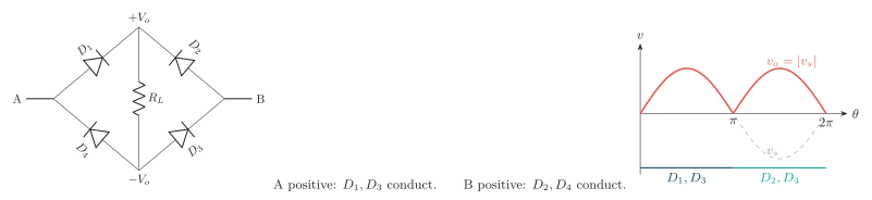
Full-wave bridge and ideal conduction/output waveforms.
For ideal diodes and , . Thus
Here is ripple factor and is ideal rectification efficiency for an load. In a practical silicon bridge, two diodes conduct in series, so while conducting. Transformer utilisation is better than in a half-wave circuit. A capacitor or LC filter can reduce ripple, but it also makes diode and transformer currents more sharply pulsed.
| Quantity | Half-wave | Full-wave bridge |
|---|---|---|
| Ripple factor | ||
| Maximum efficiency | ||
| Ripple frequency | ||
| PIV per device |
Ideal half-wave and bridge-rectifier comparison.
For a centre-tapped full-wave rectifier, PIV is per diode when is the peak of one half-secondary; this must not be confused with bridge PIV.
Single-Phase SCR-Controlled Rectifiers
Section titled “Single-Phase SCR-Controlled Rectifiers”The firing angle is the delay, measured from the natural forward-voltage zero crossing, at which the gate pulse turns on a forward- biased SCR. Changing changes the conduction interval and hence the average output.
Half-wave controlled rectifier with an load
Section titled “Half-wave controlled rectifier with an RRR load”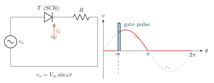
Half-wave SCR phase controller and delayed -load waveform (illustrated at ).
During , the SCR is forward biased but off. The gate pulse at turns it on; with a pure resistance, and conduction lasts only to . At the supply zero crossing, current falls below and natural commutation turns the SCR off. It remains reverse biased throughout the negative half-cycle. Hence
The average over a complete supply cycle is
Full-wave circuits: the load distinction
Section titled “Full-wave circuits: the load distinction”For a full-wave centre-tapped circuit, alternate SCRs are fired at and . A bridge may use two SCRs plus two diodes (half-controlled) or four SCRs (fully controlled).
For a pure load, load current reaches zero at every supply zero crossing. Two identical positive output pulses occur per cycle:
For a fully controlled four-SCR bridge with a sufficiently inductive load, current is assumed continuous. Each diagonal pair conducts for radians, including an interval in which output voltage is negative:
| Feature | Half-wave | Half-controlled bridge | Fully controlled bridge |
|---|---|---|---|
| Power devices | One SCR | Two SCRs and two diodes | Four SCRs |
| Output use | One half-cycle | Both half-cycles | Both half-cycles |
| Ripple frequency | |||
| Average-output sign | Non-negative | Non-negative | Positive or negative with continuous current and an active load |
| Regeneration | No | No | Possible |
| Control/complexity | Lowest | Moderate | Greatest |
Single-phase controlled-rectifier comparison.
Increasing reduces average output and usually worsens input power factor and harmonic distortion. Full-wave conversion gives higher output, higher ripple frequency and easier filtering than half-wave conversion.
For completeness, industrial high-power converters commonly use three phases. With the phase-to-neutral peak and the line-to-line RMS voltage, ideal continuous-current averages are
The three-pulse circuit uses three SCRs; the six-pulse bridge uses six SCRs and produces lower output ripple than a single-phase converter.
Linear and Switched-Mode Power Supplies
Section titled “Linear and Switched-Mode Power Supplies”A linear supply transforms at mains frequency, rectifies and filters, then operates a series-pass device in its active region. An SMPS rectifies where necessary, switches energy at high frequency, transfers or stores it in magnetic components, rectifies/filters the output and closes a feedback loop around duty ratio.
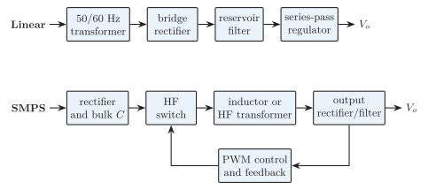
Energy and control flow in linear and switched-mode supplies.
For a linear regulator, ignoring quiescent current,
For ideal continuous-conduction switching converters with duty ratio ,
A forward converter transfers energy to the secondary while its switch is on; a flyback stores energy in magnetising inductance while on and delivers it to the secondary while off. Buck, boost and buck–boost stages are normally non-isolated; flyback, forward and bridge-derived converters can provide galvanic isolation.
| Property | SMPS | Linear supply |
|---|---|---|
| Efficiency | Typically – or higher | Often – when the voltage drop is large |
| Size and mass | Small high-frequency magnetics; high power density | Bulky 50/60-Hz transformer and heat sink |
| Conversion range | Step-down, step-up, inversion, wide input and multiple isolated outputs | Mainly step-down; constrained by dropout and dissipation |
| Heat | Low when switching and magnetic losses are controlled | High pass-device loss for large |
| Noise/EMI | Switching ripple and conducted/radiated EMI require filtering and careful layout | Very low switching noise and EMI |
| Complexity | Controller, compensation, gate drive, magnetics and protection | Simple regulator; easier design and fault finding |
| Best use | Computers, chargers, telecom and portable/high-power equipment | Precision analog, audio, laboratory and very low-noise rails |
SMPS and linear power-supply comparison.
Practical SMPS design adds an input fuse, MOV and inrush limiter, common- and differential-mode EMI filters, cycle-by-cycle current limiting, snubbers or clamps, overvoltage and thermal shutdown, safe bulk-capacitor discharge, and adequate isolation creepage and clearance. Feedback crossing an isolation barrier commonly uses an optocoupler or isolated controller.
Protection from Electrical Hazards
Section titled “Protection from Electrical Hazards”Electrical safety is the coordinated use of insulation, enclosures, earthing, automatic disconnection, isolation, energy limiting and safe work practices to prevent shock, burns, fire and equipment damage in normal use and under a credible single fault.
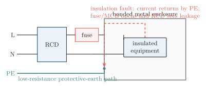
Layered Class-I protection: insulation, enclosure, PE, overcurrent protection and residual-current detection.
| Measure | Protective action |
|---|---|
| Basic/reinforced insulation and enclosure | Prevent contact with live parts; use adequate creepage, clearance, flame resistance and an appropriate IP rating. Class II equipment uses double/reinforced insulation and no PE. |
| Protective earthing (Class I) | Bonds accessible metal to PE. A live-to-case fault follows a low-resistance path and operates the protective device rather than leaving the case hazardous. |
| Fuse or MCB | Interrupts overload and short-circuit current to protect wiring and prevent fire. It is not sensitive enough to replace shock protection. |
| RCD/ELCB | Compares live and neutral currents and disconnects on residual earth leakage. A RCD is commonly used as additional personal protection, but it does not replace a fuse/MCB, insulation or PE. |
| Isolation transformer/SELV | Provides galvanic separation and limits available voltage/current, removing a direct mains-to-earth return path for a single secondary contact. |
| Surge and thermal protection | MOV/TVS devices clamp transients; thermal cut-outs and current limiting prevent excessive energy and temperature. |
| Cable and mechanical design | Correct conductor size, strain relief, secure terminals and guarded connectors prevent overheating and exposed conductors. |
| Inspection and testing | Visual checks, earth continuity, insulation resistance, leakage and RCD tests reveal deterioration before service. |
Electrical-hazard controls and the fault each addresses.
Before maintenance: de-energise, isolate, lock out/tag out, prove dead with a verified tester, discharge stored capacitors, and use appropriate tools and PPE. Relevant product standards include IEC 62368-1 for ICT/AV equipment and IEC 61010 for measurement and laboratory equipment; installation must also follow applicable national wiring rules.