Logic Fundamentals
Digital electronics represents information with a finite set of levels. Binary systems use two logic states, written 0 and 1. A logic value is an abstract state; the corresponding voltage range depends on the logic family.
Number Systems and Binary Representation
Section titled “Number Systems and Binary Representation”For radix , a positional number has value
| System | Base | Digits | Main use |
|---|---|---|---|
| Binary | , 1 | Native representation of logic and storage | |
| Octal | –7 | Compact grouping of three binary bits | |
| Decimal | –9 | Human-readable quantities | |
| Hexadecimal | –9, A–F | Compact grouping of four binary bits |
Number systems used in digital electronics.
Conversion rules.
Section titled “Conversion rules.”-
To convert an integer from decimal to base , divide repeatedly by and read the remainders from last to first.
-
To convert a decimal fraction, multiply repeatedly by and read the integer parts in order. A non-terminating result must be rounded to a stated number of places.
-
For binary–octal conversion, group bits in threes about the radix point. For binary–hexadecimal conversion, group them in fours.
An -bit word has distinct patterns. Their interpretation depends on the chosen code.
| Representation | Range for bits | Zero | Negative-value rule |
|---|---|---|---|
| Unsigned | to | one | Not available |
| Sign magnitude | to | two | Set sign bit to 1 |
| One’s complement | to | two | Complement every bit |
| Two’s complement | to | one | Complement and add 1 |
Common binary integer representations.
For an -bit two’s-complement word ,
To form , invert all bits of and add 1, discarding any carry beyond the word. For example, in eight bits,
Sign extension copies the sign bit into new high-order positions; zero extension is correct only for unsigned values.
Binary-coded decimal (BCD) stores each decimal digit separately in four bits. Thus , whereas ordinary binary gives . The six patterns 1010–1111 are invalid BCD digits.
Basic Logic Gates
Section titled “Basic Logic Gates”In positive logic, the higher specified voltage range represents 1 and the lower range represents 0. The intermediate voltage interval is normally undefined, not a third state.
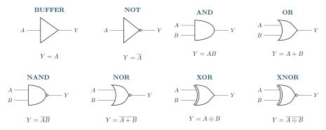
Symbols and Boolean expressions of the basic logic gates. An output bubble denotes inversion; XOR has an additional curved input line.
| Gate | Expression | Output condition |
|---|---|---|
| BUFFER | follows the input | |
| NOT | 1 when | |
| AND | 1 only when every input is 1 | |
| OR | 1 when any input is 1 | |
| NAND | complement of AND | |
| NOR | complement of OR | |
| XOR | 1 when the inputs differ | |
| XNOR | 1 when the inputs agree |
Boolean functions of the basic gates.
Complete two-input truth table.
Boolean Algebra
Section titled “Boolean Algebra”Boolean variables take values in . Addition denotes OR, multiplication denotes AND, and an overbar denotes NOT.
Core Boolean identities.
| Law | OR form | AND form |
|---|---|---|
| Identity | ||
| Null | ||
| Idempotent | ||
| Complement | ||
| Involution | — | |
| Commutative | ||
| Associative | ||
| Distributive | ||
| Absorption | ||
| De Morgan |
The principle of duality interchanges with multiplication and 0 with 1. Every valid identity therefore has a valid dual. De Morgan’s laws also show why NAND and NOR are universal:
Logic Expressions and Truth Tables
Section titled “Logic Expressions and Truth Tables”A truth table defines a function row by row. An expression may be written in two canonical forms:
-
sum of minterms: OR the product term for every row where ; write ;
-
product of maxterms: AND the sum term for every row where ; write .
In a minterm, use the uncomplemented variable for a row value 1 and the complemented variable for 0. In a maxterm the convention is reversed.
For example,
has a 1 in rows 001, 010, 011, 101 and 111. Its canonical SOP is
Karnaugh-map simplification
Section titled “Karnaugh-map simplification”Adjacent K-map cells differ in one variable. Group 1s for SOP or 0s for POS in rectangles containing cells. Groups may wrap across an edge, overlap, and should be as large as possible. A variable disappears from a term when it changes within a group.
| A BC | 00 | 01 | 11 | 10 |
| 0 | 0 | 1 | 1 | 1 |
| 1 | 0 | 1 | 1 | 0 |
The four cells with give ; the remaining pair at gives . Hence
Do not treat diagonally touching cells as adjacent, and keep row/column order Gray-coded: 00, 01, 11, 10.
From Requirement to Circuit
Section titled “From Requirement to Circuit”-
Define input and output variables, including active-HIGH or active-LOW conventions.
-
Build the truth table and mark impossible states as don’t-cares only when the hardware guarantees they cannot occur.
-
Write canonical SOP or POS, then simplify algebraically or by K-map.
-
Select gates or a universal NAND/NOR realization and draw every inversion explicitly.
-
Verify all input rows and estimate logic depth, loading and delay.
For a combinational path with gate delays , a conservative worst-case estimate is
The physical design must also respect fan-out, noise margins, supply limits and unused-input rules of its chosen logic family.