Amplifiers
Amplifier Fundamentals and Classification
Section titled “Amplifier Fundamentals and Classification”An amplifier is an active circuit in which a small input signal controls energy drawn from a DC supply to produce a larger output signal. It does not create energy: its signal power gain is supplied by the DC source. For linear small-signal operation, the active device is biased at a quiescent point (Q point) and is operated over a region in which incremental relations are approximately linear.
Voltage, current and power gains are different port quantities:
For sinusoidal signals at resistive ports,
A voltage ratio is written as dB. Interpreting that number as a power-gain comparison requires equal reference impedances; otherwise the impedance ratio must also be included. A CE or CS voltage gain is negative because the output is inverted, whereas power gain is quoted as a positive ratio.
Amplifiers may be classified by the amplified quantity (voltage, current, transconductance, transresistance or power), coupling (RC, direct or transformer), frequency range (audio, video/baseband, IF or RF), device connection, signal level and conduction class.
Untuned Amplifiers and Coupling Methods
Section titled “Untuned Amplifiers and Coupling Methods”An untuned amplifier provides useful gain over a continuous frequency band without using an LC resonator as its selective load. Untuned does not mean infinite or perfectly flat bandwidth: coupling and bypass capacitors usually set the low-frequency limit, while device, wiring and load capacitances set the high-frequency limit.
Stages are coupled to transfer signal while satisfying requirements for DC bias isolation, bandwidth, impedance matching, power transfer, size and distortion.
RC, direct and transformer coupling
Section titled “RC, direct and transformer coupling”RC coupling
Section titled “RC coupling”An interstage capacitor passes AC but blocks DC, so adjacent Q points remain substantially independent. Its reactance increases at low frequency and forms a high-pass network with the surrounding resistances. RC coupling is cheap, compact and gives useful broadband voltage gain, but it provides poor impedance matching and is unsuitable for direct high-power transfer to a low resistance.
Direct coupling
Section titled “Direct coupling”A conductive connection passes both DC and AC, so response can extend to . It is natural in ICs, op-amps, differential stages and sensor interfaces. Its disadvantages are propagation of offset and drift, interaction of stage bias points and the possible need for level shifting.
Transformer coupling
Section titled “Transformer coupling”AC transfers magnetically while DC is isolated. For an ideal transformer,
The turns ratio can therefore present a suitable load to a transistor and a centre-tapped winding can phase-split a push-pull drive. Transformer coupling is bulky and costly; winding resistance, core loss and nonlinearity, leakage inductance and interwinding capacitance limit efficiency and bandwidth.
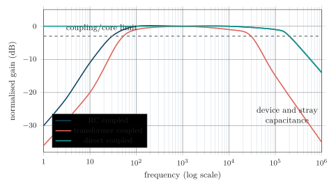
Qualitative native comparison of RC-, transformer- and direct-coupled frequency responses. Actual cutoffs depend on the circuit.
| Property | RC | Direct | Transformer |
|---|---|---|---|
| Transfers DC | No | Yes | No |
| Low-frequency limit | Coupling/bypass capacitance | Can include DC | Magnetising inductance and core |
| Stage-bias isolation | Good | Poor | Excellent |
| Impedance matching | Poor | Not inherent | Excellent by turns ratio |
| Typical use | Audio and general voltage stages | Op-amps, sensors and ICs | Power output, isolation and matching |
| Main limitation | Low- roll-off and weak power matching | Offset and thermal drift propagate | Bulk, cost, loss and restricted bandwidth |
Selection of an interstage coupling method.
CE RC-Coupled Amplifier
Section titled “CE RC-Coupled Amplifier”A common-emitter RC-coupled stage combines voltage-divider bias, a resistive collector load and capacitors that preserve DC bias while carrying the wanted AC signal.
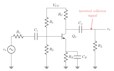
Complete loaded CE RC-coupled amplifier with input/output coupling and emitter-bypass capacitors.
| Component | Function |
|---|---|
| Establish a reasonably stiff base-bias voltage. | |
| Converts collector-current change into an inverted voltage change. | |
| Provides DC degeneration and stabilises current against and temperature variation. | |
| Bypasses over the intended AC band to recover voltage gain. | |
| Pass AC while blocking source/base and collector/load DC levels. | |
| Receives output signal power and loads for AC. |
Function of each component in the figure.
DC bias and signal operation
Section titled “DC bias and signal operation”At DC, and are open. When divider current is large compared with base current,
The Q point is chosen in the active region with enough headroom for the desired approximately symmetrical collector-voltage swing. Exact divider-bias analysis uses the Thevenin source and so that base-current loading is included.
On a positive input half-cycle, and increase. The drop across increases and falls. On the negative half-cycle the opposite occurs. The collector output is therefore amplified and shifted by approximately .
Midband small-signal gain and loading
Section titled “Midband small-signal gain and loading”At room temperature,
Let . If is an AC short, the emitter is at AC ground, and the signal is defined at the base,
With ,
Thus a finite source resistance gives the source-to-load gain
The intrinsic transistor current ratio is not the overall load-current gain : bias-network current, source attenuation and collector/load current division must be included. For RMS quantities at resistive input and output ports,
provided all port voltage/current definitions are used consistently.
Low-, mid- and high-frequency regions
Section titled “Low-, mid- and high-frequency regions”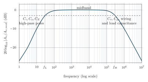
Native three-region response of a practical RC-coupled CE stage.
Low frequency
Section titled “Low frequency”As falls, rises. The input and output capacitors attenuate signal transfer, while incomplete bypass increases emitter degeneration. Useful first estimates are
Other independent sources and capacitors are set to their small-signal conditions when finding each resistance. The combined is not simply the largest individual pole when two or more poles are close.
Midband
Section titled “Midband”are approximately short circuits for signal, while device and stray capacitances are approximately open. Gain is nearly constant and the midband model leading to the equation applies.
High frequency
Section titled “High frequency”Base-emitter diffusion capacitance , collector-base capacitance , wiring capacitance and load capacitance shunt signal and introduce phase lag. In an inverting high-gain stage, Miller multiplication of is often the dominant mechanism.
At either overall cutoff,
This is a dB voltage ratio and, for the same load, one-half of midband output power. Only when may one use .
Miller effect
Section titled “Miller effect”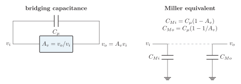
Native Miller transformation of the base-collector feedback capacitance into input- and output-referred capacitances.
Because the capacitor current is
the source sees
An approximate total input capacitance and its pole are
where . Miller effect lowers high-frequency input impedance, reduces , slows rise time (approximately for a dominant pole), and adds phase lag. It can be mitigated by a cascode, a device with smaller , lower gain per stage, or neutralisation. A lower source resistance raises the input pole but does not reduce the Miller-equivalent capacitance itself.
Power Amplifiers
Section titled “Power Amplifiers”| Definition | Concept / overview | Construction |
| Working | Derivation | Advantages |
| Disadvantages | Applications | Pitfall |
| Tip | Key point | Mnemonic |
Text is meaning-coded too: definition, key/important, advantage, disadvantage, application. Each block also has a distinct icon, so the meaning survives greyscale printing.
What is a Power Amplifier?
Section titled “What is a Power Amplifier?”A power amplifier is a large-signal amplifier — usually the final stage of a multistage system — whose job is to deliver a large amount of power to a low-impedance load such as a loudspeaker, motor, servo, or antenna. It is designed to maximise output power and efficiency, not voltage gain.
-
Large-signal operation: it handles big voltage and current swings, so the device moves over a large part of its load line (unlike a small-signal voltage amplifier).
-
Provides current/power gain: the preceding voltage amplifier supplies a large voltage; the power stage supplies the current needed to drive a low- load.
-
Key design concerns: output power, efficiency , power dissipation / heat (heat sinks, thermal runaway), distortion (large-signal non-linearity), and impedance matching to the load.
-
Figure of merit — efficiency:
the rest of the DC power becomes heat in the device.
| Voltage (small-signal) amp | Power (large-signal) amp | |
|---|---|---|
| Goal | high voltage gain | high output power + efficiency |
| Signal | small | large |
| Load line | small portion used | large portion used |
| Load | high | low (e.g. 4 –8 speaker) |
| Output power | milliwatts | watts |
| Main worry | gain, noise | heat, efficiency, distortion |
How power amplifiers are classified
Section titled “How power amplifiers are classified”-
By conduction angle / biasing Class A (), Class B (), AB, C ().
-
By operating mode Class D (switching / PWM).
-
By coupling RC-coupled, transformer-coupled, direct-coupled.
-
By frequency audio-frequency (AF) or radio-frequency (RF).
The conduction angle = the part of the input cycle during which the output device actually conducts current.
One-cycle waveform comparison
Section titled “One-cycle waveform comparison”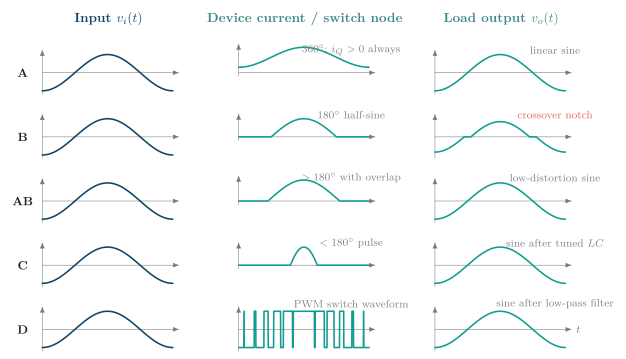
Conduction intervals and representative output waveforms for amplifier classes A, B, AB, and C.
Class A Amplifier
Section titled “Class A Amplifier”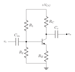
Series-fed class-A power-amplifier circuit.
Series-fed (RC-coupled) Class A stage with voltage-divider bias.
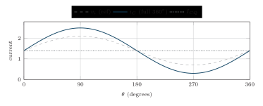
Class-A collector-current and output-voltage waveforms over a complete cycle.
never reaches zero — conduction over the whole cycle.
Class A push–pull (transformer-coupled)
Section titled “Class A push–pull (transformer-coupled)”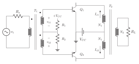
Transformer-coupled push-pull class-A amplifier.
The transformer-coupled Class A push–pull amplifier drives alternate halves of the output transformer from the two active devices.
Class B Amplifier
Section titled “Class B Amplifier”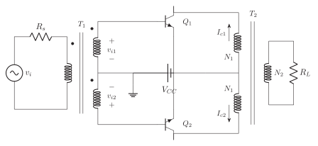
Transformer-coupled push-pull class-B amplifier.
The transformer-coupled push–pull Class B amplifier uses alternate half-cycles to drive the output transformer.
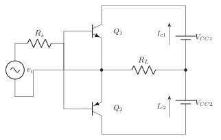
Complementary-symmetry class-B output stage.
The complementary-symmetry Class B stage uses opposite transistor polarities to source and sink load current.
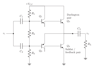
Quasi-complementary class-B output stage.
In the quasi-complementary Class B stage, – form the upper Darlington pair while – form the lower complementary-feedback (Sziklai) pair.
The Sziklai pair combines a small PNP driver with an NPN power transistor to behave as a high-gain PNP-like composite device.
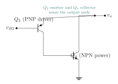
Complementary-feedback Sziklai transistor pair and its composite PNP equivalent.
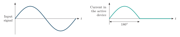
Class-B device-current waveforms and reconstructed output.
In Class B operation, each active device conducts for exactly of the input cycle.
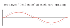
Class-B crossover distortion caused by the transistor dead zone.
Class AB Amplifier
Section titled “Class AB Amplifier”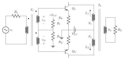
Transformer-coupled class-AB output stage.
In the transformer-coupled Class AB stage, establish forward bias and stabilises the quiescent current.
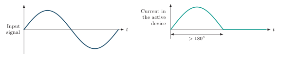
Class-AB device-current waveforms and reconstructed output.
Class AB device current lasts slightly more than because a small quiescent current remains at zero input.
Class C Amplifier
Section titled “Class C Amplifier”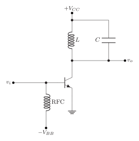
Class-C amplifier with a tuned collector load.
In the tuned-mode Class C amplifier, the RFC supplies negative DC base bias while blocking RF, and the parallel tank selects the output sinusoid.
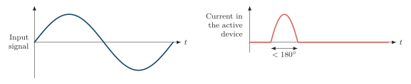
Class-C current pulses and tuned-load output waveform.
Class C device current is a narrow pulse with conduction angle less than .
Class D Amplifier
Section titled “Class D Amplifier”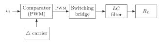
Class-D switching-amplifier signal chain.
Class D signal chain: PWM switching bridge filter load.
Other switching classes (E, F)
Section titled “Other switching classes (E, F)”Class E and Class F are switching power amplifiers offering very high efficiency, used at very high frequencies where the switching time is comparable to the duty time.
Power Amplifier Characteristics
Section titled “Power Amplifier Characteristics”Efficiency
Section titled “Efficiency”= AC power delivered to the load, = DC input power (also called conversion efficiency).
Harmonic Distortion (five-point method)
Section titled “Harmonic Distortion (five-point method)”Device non-linearity adds harmonics, and distortion grows with signal level. From five sampled output-current points () the Fourier amplitudes are:
Individual and total harmonic distortion:
Fundamental power ; total output power
Thermal Management
Section titled “Thermal Management”-
Average device dissipation: .
-
The limiting factor is the maximum collector junction temperature. Above a rated case temperature the allowed derates linearly to zero at the maximum case temperature (C for silicon; Si withstands more than Ge).
-
Improve power handling with heat sinks (large metal case area) or thermoelectric (Peltier) coolers — solid-state heat pumps that move heat against the temperature gradient.
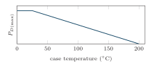
Power-transistor dissipation derating with case temperature.
Silicon power-transistor derating curve.
All Classes — Comparison
Section titled “All Classes — Comparison”| Class | Conduction | Distortion | Typical use | |
|---|---|---|---|---|
| A | % / 50% | lowest | preamp, hi-fi small-signal | |
| AB | –78% | low (no crossover) | audio output (common) | |
| B | % | crossover | audio push–pull | |
| C | up to 90% | high (needs tank) | RF/IF, transmitters | |
| D | switch (PWM) | low (filtered) | audio, motor drive | |
| E,F | switching | very high | — | very-high-frequency |
Feedback Amplifiers
Section titled “Feedback Amplifiers”Feedback returns a fraction of an amplifier output to its input. Negative (degenerative) feedback subtracts the returned signal from the source and is used to control linear-amplifier behavior. Positive (regenerative) feedback reinforces the source and is used deliberately in oscillators, hysteresis and switching; excessive positive feedback makes a linear stage unstable.
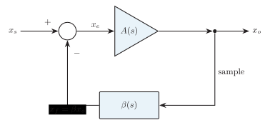
Native negative-feedback block diagram with an explicit subtracting input. Changing the lower sign changes the algebra to positive feedback.
Closed-loop gain and desensitivity
Section titled “Closed-loop gain and desensitivity”With the sign in the figure,
Therefore
The generally complex, frequency-dependent product
is the loop gain; is the return difference. When and the loop phase still represents negative feedback, . For positive feedback under the same algebraic convention,
so the two denominators must not be interchanged.
For scalar and fixed , logarithmic differentiation gives
Qualified effects of negative feedback
Section titled “Qualified effects of negative feedback”| Property | Effect in the useful negative-feedback band |
|---|---|
| Gain | Reduced by the return difference , but made more predictable; high loop gain exchanges excess open-loop gain for accuracy. |
| Bandwidth | For a stable single-dominant-pole stage and nearly constant , and , so gain-bandwidth product is approximately conserved. These are not multipole identities. |
| Distortion | Nonlinear products generated inside the effective forward-path loop are reduced approximately by $1+ |
| Noise | Some noise generated inside the enclosed forward path is reduced at the output relative to signal. Source noise and feedback-network thermal noise are not automatically reduced, and a wider noise bandwidth may increase total noise. |
| Stability and transient response | Parameter stability improves, but accumulated phase lag can make the returned signal regenerative. Inadequate phase margin produces ringing or oscillation, so loop stability must be checked separately. |
| Impedance | Determined by input mixing and output sampling: there is no single rule that both impedances always rise or always fall. |
What negative feedback changes, and the necessary qualification.
Four feedback topologies
Section titled “Four feedback topologies”Topology is decoded by two independent questions:
-
Is feedback mixed with the input in series as a voltage, or in shunt as a current?
-
Is output voltage sampled across the port (shunt sampling), or output current sampled through the port (series sampling)?
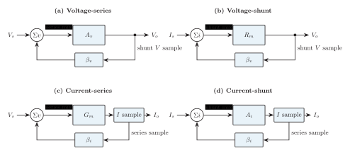
Native topology decoder. The input symbol distinguishes series voltage from shunt current mixing; the output branch distinguishes voltage from current sampling.
Let in a frequency band where feedback is negative and may be treated as a positive scalar magnitude. The impedance rules and stabilised gain quantities are:
| Topology | Amplifier quantity | Sample–mix | ||
|---|---|---|---|---|
| Voltage-series | Voltage–series (shunt–series) | |||
| Voltage-shunt | Voltage–shunt (shunt–shunt) | |||
| Current-series | Current–series (series–series) | |||
| Current-shunt | Current–shunt (series–shunt) |
Feedback topology, gain quantity and impedance effects.
The memory rule follows directly: series input raises ; shunt input lowers it; voltage sampling lowers ; current sampling raises it. Series mixing makes the source overcome a feedback voltage, while shunt mixing adds a current path. Voltage sampling tends toward a stiff voltage source and current sampling toward a stiff current source.
Advantages of negative feedback are accurate gain, useful impedance control, wider bandwidth in common dominant-pole designs, and reduced enclosed distortion and some internal noise. Its costs are reduced gain, extra network noise/loading and the possibility of ringing or oscillation. Applications include op-amps, audio and instrumentation amplifiers, active filters, regulators and communication signal paths.
Differential Amplifiers
Section titled “Differential Amplifiers”A differential amplifier is a direct-coupled two-input stage that amplifies the difference between its inputs while rejecting a signal common to both. It is the usual input stage of an op-amp and a basic interface for balanced sensors and communication lines.
Define the input quantities before deriving a gain:
so that
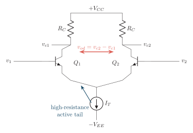
Native matched BJT differential pair with equal collector loads and a constant-current tail. Either collector or their difference may be output.
At balance, , matched devices divide equally, collector drops are equal and ideally. For positive , current rises and falls; current falls and rises. The pair therefore steers an almost constant tail current between its branches.
For common-mode drive , both branch currents try to move in the same direction. The tail element then develops degenerative emitter voltage. A high small-signal tail resistance strongly opposes total-current change. Matched collector changes cancel in an ideal double-ended output, while a single-ended output and practical mismatch leave finite common-mode gain.
Differential and common-mode half-circuits
Section titled “Differential and common-mode half-circuits”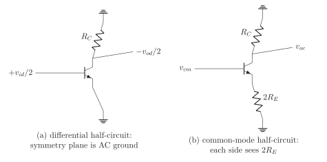
Native half-circuit views for a resistor-tail pair. An active tail replaces by a much larger incremental resistance.
Differential gain, common-mode gain and CMRR
Section titled “Differential gain, common-mode gain and CMRR”Assume matched devices and loads, large , large transistor , and
at room temperature. With and ,
Consequently,
For the output polarities shown in the figure,
With a shared resistor and a single-collector output,
The common-mode rejection ratio must compare gains measured at the same output:
Active tails and practical errors
Section titled “Active tails and practical errors”A large resistor improves CMRR but consumes excessive DC voltage. A transistor current sink supplies the required DC current while presenting high small-signal output resistance. For a Zener-referenced sink,
A current mirror uses a diode-connected reference transistor to establish and a matched output transistor to sink approximately the same current. In a representative dual-supply arrangement,
Finite , Early effect, device mismatch, temperature difference and compliance voltage limit accuracy. Zener noise and drift are additional limits of the Zener source.
| Tail | DC setting | Incremental resistance/CMRR | Main limitation |
|---|---|---|---|
| Resistor | Supply and | Moderate; rises only with physical resistance | Large resistance needs large voltage |
| Zener sink | , and | High; low common-mode gain | Zener noise, drift and compliance |
| Current mirror | Reference branch and matching | High; compact and IC-friendly | Mismatch, finite , Early effect and compliance |
Tail-network comparison for a differential pair.
Practical limitations include input offset from device/load mismatch, input bias and offset currents
finite common-mode input range, tail-source compliance and collector saturation headroom. Large steers almost all tail current to one branch and violates the small-signal model. Matched devices, symmetric layout, equal source resistances and trimming reduce error. High CMRR rejects common hum, balanced-line pickup, sensor-lead interference and ground-potential variation.
Cascode Amplifiers
Section titled “Cascode Amplifiers”A cascode is one composite stage formed by stacking a transconductance input device below a current-buffer device: CE followed by CB for BJTs, or CS followed by CG for FETs. The upper device keeps the lower device’s collector or drain at nearly constant AC voltage while transferring signal current to a high-resistance output node.
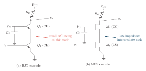
Native CE–CB and CS–CG cascodes. The upper device shields the input device from the large output-voltage swing.
In the BJT form, converts into collector-current variation. The emitter of common-base presents low incremental resistance, so the collector voltage changes little. conveys the current to , which produces an amplified inverted output. In the MOS form, common-gate similarly holds the drain nearly fixed and transfers its drain current to .
Miller suppression, gain and port resistances
Section titled “Miller suppression, gain and port resistances”For an ordinary inverting stage, a feedback capacitance appears at its input as . In a cascode, the relevant local gain from the lower device input to its collector/drain is small. The voltage across or therefore changes little, greatly reducing Miller multiplication. The result is lower effective input capacitance, higher upper cutoff and better reverse isolation. Output-node capacitance can still form a limiting pole.
The lower device supplies transconductance and the upper device supplies isolation and high intrinsic output resistance. A useful loaded estimate is
For a BJT cascode, in parallel with its bias network. For a MOS cascode, gate input resistance is ideally very high and is limited by bias resistance and leakage. Looking into the lower device’s collector/drain, the upper CB/CG device presents a low resistance of order ; looking into the final output, the cascode resistance is high as shown above.
Advantages are low Miller effect, wide bandwidth, high reverse isolation, high output resistance and potentially high gain. Costs are extra device and bias circuitry, greater voltage headroom, reduced low-supply output swing, added noise and a possible high-impedance output pole. Applications include RF and IF amplifiers, low-noise and wideband front ends, oscilloscope inputs, op-amp gain stages, active loads and high-output-resistance current mirrors.
Differential pair versus cascode
Section titled “Differential pair versus cascode”| Feature | Differential pair | Cascode |
|---|---|---|
| Primary purpose | Amplify and reject common mode | Suppress Miller feedback, isolate ports and raise output resistance |
| Input structure | Two signal inputs sharing one tail current | One principal signal input; upper device receives fixed bias |
| Signal mechanism | Steers tail current between two branches | Transfers one device’s signal current through a CB/CG buffer |
| Key figure of merit | Differential gain, common-mode gain and CMRR | Bandwidth, reverse isolation, gain and output resistance |
| Headroom | Tail source and both input devices need compliance | Stacked devices need extra voltage and reduce output swing |
| Typical use | Op-amp/instrumentation and balanced-input front end | RF, wideband, high-gain or high-output-resistance stage |
Differential and cascode amplifiers solve different problems.
A cascode must also be distinguished from an ordinary cascade. In a cascode, devices share one current path and the intermediate voltage swing is intentionally small. In a cascade, the output of one complete stage drives another and stage gains multiply; each inverting stage may retain its own Miller limitation.
Supplementary Amplifier Topics
Section titled “Supplementary Amplifier Topics”The following topics provide complementary derivations, circuit interpretations, comparison tables and worked design checks for differential, operational and feedback amplifiers.
Differential Amplifiers
Section titled “Differential Amplifiers”A differential amplifier is a direct-coupled, two-input stage that amplifies the input difference while rejecting a signal common to both inputs. For the polarity ,
It is the standard input stage of op-amps and instrumentation amplifiers.
It is useful to separate any pair of input voltages into differential and common-mode components:
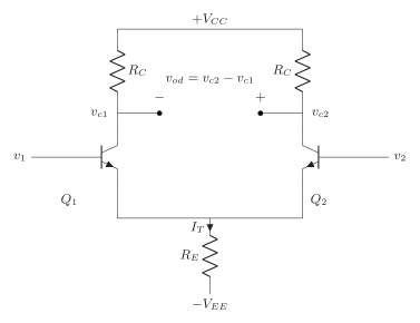
Matched BJT differential amplifier with equal collector loads and a shared resistor tail. A current-source or current-mirror tail is preferred in practical high-CMRR stages.
At balance, matched transistors divide the tail current equally and their collector voltages are equal. A positive steers current toward : falls while rises. Common-mode drive attempts to change both currents together; the shared tail impedance develops degenerative feedback and opposes that change.
At room temperature, with large transistor and negligible ,
For equal collector resistors and the indicated output polarities,
The common-mode rejection ratio is
For the same single-ended collector output,
With matched devices and equal collector resistors, the double-ended common-mode gain is ideally zero (), so rigorous CMRR comparison should keep output convention explicit.
Operational Amplifiers
Section titled “Operational Amplifiers”An operational amplifier (op-amp) is a very-high-gain, DC-coupled, differential voltage amplifier. In linear open-loop operation,
where is the open-loop differential gain and . This relation is valid only while the output remains in the unsaturated range.
Direct coupling allows response down to , but it also means input offset and drift appear at the output after gain. The op-amp symbol, power pins and internal stage concept are shown below.
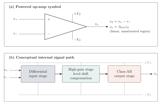
Powered op-amp symbol and a conceptual internally compensated three-stage signal path with explicit supply distribution.
Practical and Ideal Models
Section titled “Practical and Ideal Models”At low frequency, a practical op-amp can be modeled by finite differential input resistance , a dependent source , and non-zero output resistance . The ideal model is the limiting case
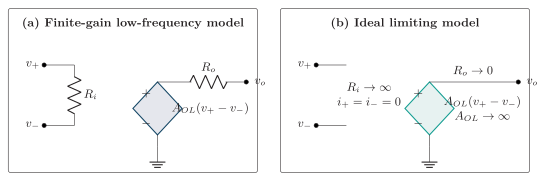
Practical and ideal op-amp terminal models. The finite-gain VCVS is ground referenced and followed by series ; the ideal limit has , , and .
| Parameter | Ideal | Practical trend | Consequence |
|---|---|---|---|
| Open-loop gain | to (device dependent) | Closed-loop gain has finite-gain error. | |
| Input resistance | to | Input currents are small, not exactly zero. | |
| Output resistance | typically ohms to tens of ohms | Load changes cause finite output drop. | |
| Bandwidth / GBW | finite, compensation dependent | Gain and phase vary with frequency. | |
| Slew rate | finite ( to hundreds of ) | Large-signal slope limit can distort waveforms. | |
| Offsets and drift | finite, temperature/time dependent | DC accuracy needs offset/drift budgeting. |
Ideal assumptions and practical interpretation (order-of-magnitude only).
Frequency Response, Loop Gain and Closed-Loop Accuracy
Section titled “Frequency Response, Loop Gain and Closed-Loop Accuracy”A compensated op-amp is often approximated by a dominant-pole model:
Beyond the pole, the open-loop magnitude falls at about until higher poles appear. In the one-pole region,
is an approximation, where is the unity-gain frequency.
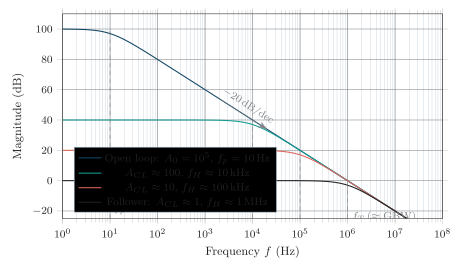
Exact magnitudes for the one-pole model with (), , and . Closed-loop bandwidth follows the gain–bandwidth product to the accuracy of this model.
For a standard negative-feedback amplifier with feedback factor ,
Slew Rate, Full-Power Bandwidth and Settling
Section titled “Slew Rate, Full-Power Bandwidth and Settling”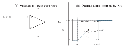
Slew-rate measurement with a voltage-follower step test. The large-signal output needs to traverse the step.
In internally compensated op-amps, slew-rate limiting is set by finite internal current charging/discharging the compensation capacitor:
If required output slope exceeds , distortion occurs even when small-signal bandwidth seems adequate.
For a step response with final value and step size , settling time to error band is formally defined as
Typical data-sheet bands are (0.1%) or (0.01%). Practical settling depends on step amplitude, slew interval, small-signal poles/zeros, phase margin and load.
CMRR, PSRR, Offsets and Drift
Section titled “CMRR, PSRR, Offsets and Drift”CMRR is meaningful only for valid common-mode input range and linear output range. Practical CMRR changes with frequency and source imbalance.
PSRR is often specified through input-referred offset sensitivity, (smaller is better). Some data sheets use the reciprocal ratio in dB. Regardless of convention, stronger supply rejection is better and is frequency dependent.
Input offset voltage is the differential DC voltage needed to force . Offset drift is its change with temperature/time. Broadly, general parts may sit around millivolts, while precision parts can be in the microvolt range.
Op-Amp Categories and Application-Specific Forms
Section titled “Op-Amp Categories and Application-Specific Forms”| Category | Emphasis | Typical trade-off or caution |
|---|---|---|
| General-purpose | Balanced cost, gain, speed, input performance | Does not maximize any single metric. |
| High-speed | High GBW, high SR, fast settling | Layout sensitivity, power and noise penalties. |
| Precision | Very low , drift, bias errors; high DC accuracy | Often lower speed and higher cost. |
| Power | High output current/voltage, protection features | Thermal design and stability with reactive loads. |
| Comparator (dedicated) | Fast open-loop switching to logic states | Not interchangeable with linear op-amp behavior. |
Common op-amp categories (ranges are broad and device dependent).
Instrumentation Amplifier (Three-Op-Amp Topology)
Section titled “Instrumentation Amplifier (Three-Op-Amp Topology)”An instrumentation amplifier is a circuit category, not merely one op-amp type. It combines very high input impedance, accurate differential gain and strong common-mode rejection.
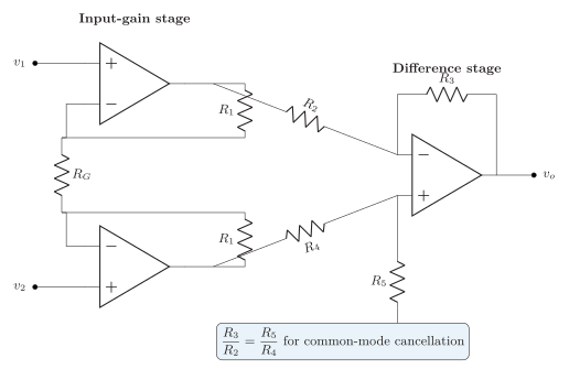
Three-op-amp instrumentation amplifier. sets the first-stage differential gain without loading either input, and matched subtractor ratios reject the first-stage common-mode component.
If the difference-stage resistor ratios are matched , then
Single-resistor gain setting by is a major practical advantage in precision sensor interfaces.
Isolation Amplifier
Section titled “Isolation Amplifier”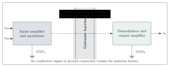
Isolation-amplifier signal path with two electrically independent ground domains. The dashed arrow denotes encoded information transfer, not a conductive connection across the barrier.
An isolation amplifier transfers the measurement signal across a galvanic barrier so that input and output grounds remain electrically separated for safety and ground-loop control. Coupling across the barrier is commonly transformer, optical, or capacitive. Specifications include isolation voltage, leakage, CMRR versus frequency, and linearity.
Feedback in Amplifiers
Section titled “Feedback in Amplifiers”A feedback amplifier returns a controlled fraction of output to the input summing mechanism. Let be source signal, be the internal error (driving) signal, be output, and be feedback.
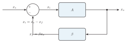
General negative-feedback loop with source signal , error signal , output , and feedback .
With a real-positive sign convention:
If forward gain is , then
and for regenerative form
Define loop gain and desensitivity factor
In the useful negative-feedback band, is typically large and positive in its real part, but in general it is complex and frequency dependent.
Barkhausen Condition and Stability Meaning
Section titled “Barkhausen Condition and Stability Meaning”Under the above denominator convention, the linear oscillation boundary is
which is equivalent to
This is a condition for marginal linear oscillation. It is not proof of physically infinite output; practical oscillators settle by nonlinear amplitude limiting.
Desensitivity, Gain Stability and Sensitivity
Section titled “Desensitivity, Gain Stability and Sensitivity”For treated as constant with respect to plant variation,
leads to
Hence sensitivity of closed-loop gain to open-loop gain is
For high loop gain ( in the intended band),
so closed-loop gain is mainly set by the feedback network.
Bandwidth and Frequency-Response Trade-Off
Section titled “Bandwidth and Frequency-Response Trade-Off”For a dominant-pole or approximately constant loop-gain region, negative feedback widens useful bandwidth roughly by while reducing midband magnitude by a similar factor:
These are one-pole approximations, not universal equalities. As loop gain is pushed upward, phase margin and stability must be rechecked.
Distortion and Noise Caveats
Section titled “Distortion and Noise Caveats”If nonlinear distortion or internally generated noise is injected inside the high-loop-gain region, its output contribution is reduced approximately by :
But feedback does not magically remove source/input noise or thermal noise from the feedback network itself, and wider closed-loop bandwidth can increase total integrated output noise.
Four Feedback Topologies
Section titled “Four Feedback Topologies”Naming is used in two ways:
-
Functional order: sample-mix (voltage/current sample at output, then series/shunt mixing at input).
-
Connection order: input-output, often written series-shunt, shunt-shunt, series-series, shunt-series.
Map carefully between them to avoid label reversal.
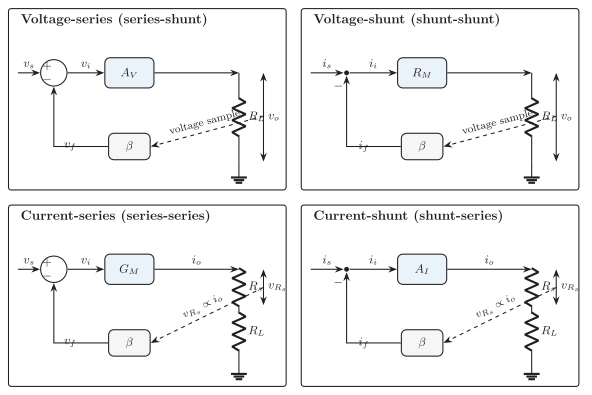
The four feedback topologies. Voltage sampling measures across the load; current sampling uses a series sense resistor carrying the load current. Dashed arrows represent measured information, while solid arrows show the forward and feedback signal paths.
| Functional name | Connection name | Transfer type | Core closed-loop form | ||
|---|---|---|---|---|---|
| Voltage-series | Series-shunt | Voltage gain | |||
| Voltage-shunt | Shunt-shunt | Transresistance | |||
| Current-series | Series-series | Transconductance | |||
| Current-shunt | Shunt-series | Current gain |
Feedback topology matrix using in the intended negative-feedback band.
Loaded/Open-Circuit/Short-Circuit Gain Notes
Section titled “Loaded/Open-Circuit/Short-Circuit Gain Notes”Use the appropriate open-loop transfer for each topology before applying .
-
Voltage-series: loaded ; if needed, with open-circuit gain .
-
Voltage-shunt: loaded transresistance ; often with open-circuit transresistance .
-
Current-series: loaded transconductance ; common model where is short-circuit transconductance.
-
Current-shunt: current gain from the loaded current model.
These loaded relations are model-dependent approximations; keep open-circuit and short-circuit definitions distinct in derivations.
Typical Realizations
Section titled “Typical Realizations”-
Voltage-series: emitter follower, source follower, non-inverting op-amp.
-
Voltage-shunt: collector-to-base resistor feedback CE stage, inverting op-amp.
-
Current-series: CE/CS with unbypassed emitter/source resistor.
-
Current-shunt: current-amplifier forms using series output current sensing and shunt current mixing.
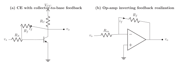
Classical voltage-shunt (shunt-shunt) realizations: a CE stage with collector-to-base resistor feedback and the op-amp inverting amplifier.
Practical Topology Identification (Robust Method)
Section titled “Practical Topology Identification (Robust Method)”Quick short/open tests are easy to misuse. Prefer structural inspection first:
-
Output sample network connected across output node/load implies voltage (shunt) sampling.
-
Output sample element inserted in load path implies current (series) sampling.
-
Feedback signal inserted in series with source/input loop implies series mixing.
-
Feedback current returning to the same summing input node implies shunt mixing.
A circuit-zeroing test can be used only with topology-aware assumptions about controlled sources and loading.