Operational Amplifiers
An operational amplifier (op-amp) is a direct-coupled, very-high-gain differential voltage amplifier with two inputs and one single-ended output:
It was named for its original use in analog computers to perform addition, subtraction, integration and differentiation.
Internal Arrangement and Ideal Model
Section titled “Internal Arrangement and Ideal Model”The signal passes through a differential input stage (high input resistance, first gain and common-mode rejection), a high-gain and level-shift stage (most of and dominant-pole compensation), and a class-AB push-pull output stage (low output resistance and load-current drive). Direct coupling permits amplification down to DC, but also allows offset and temperature drift to reach the output.
| Parameter | Ideal | Typical A741 |
|---|---|---|
| Open-loop gain | () | |
| Input impedance | ||
| Output impedance | ||
| Unity-gain bandwidth | ||
| CMRR | about | |
| Slew rate | ||
| Input offset voltage | about | |
| Input bias/offset currents | about |
Ideal and representative practical op-amp characteristics.
The low-frequency practical model has a large differential resistance , a controlled source , and a non-zero series output resistance . Its gain falls with frequency, output voltage and current are bounded by the supplies and output stage, and large-signal speed is limited by slew rate. The ideal model is the limiting case
Practical Performance Parameters
Section titled “Practical Performance Parameters”Open-loop gain :
ratio without feedback. Large loop gain makes a feedback-set closed-loop gain accurate, but falls with frequency.
Input and output impedance:
high avoids source loading and low makes output voltage insensitive to load. Voltage feedback generally raises the non-inverting closed-loop input impedance and lowers output impedance; both improvements diminish as loop gain falls at high frequency.
Common-mode rejection ratio:
if , then
High CMRR rejects hum or interference appearing equally at both inputs.
Power-supply rejection ratio:
under the common input-referred convention,
Higher is better. A data sheet may instead quote supply sensitivity in , for which smaller is better.
Input offset and currents:
is the differential DC voltage required to force zero output. The input-current quantities are
Offset is multiplied approximately by noise gain, while currents create errors in source resistances. Making the DC resistance seen by both inputs equal cancels much of the average-bias-current error, not the mismatch .
Drift and noise:
offset and current change with temperature and time; voltage/current noise limit the smallest usable signal. These are decisive in precision DC and sensor interfaces.
Input/output ranges:
the common-mode input range, output swing, output-current limit and supply rails must all be respected. Rail-to-rail labels do not imply zero headroom at every load.
Frequency and Large-Signal Response
Section titled “Frequency and Large-Signal Response”For a dominant-pole compensated op-amp,
At the open-loop magnitude is below ; beyond it the response falls at about . The unity-gain or transition frequency satisfies . Thus
where is the closed-loop noise gain. The familiar is valid only when signal gain and noise gain coincide.
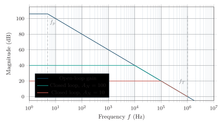
Dominant-pole open-loop response and the gain–bandwidth trade-off.
The slew rate is the maximum large-signal output slope:
For , the maximum required slope is ; hence the full-power bandwidth is
This is distinct from small-signal bandwidth. The usable frequency is bounded by the stricter of GBW, slew rate, swing and output-current requirements.
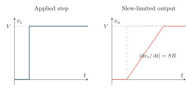
A large step cannot make the output change faster than the slew rate.
After a step, settling time is the time required to enter and remain inside a stated error band such as , or one-half LSB. It may contain a slew interval, linear settling and ringing due to limited phase margin; therefore settling time is not interchangeable with either bandwidth or slew rate.
Basic Closed-Loop Configurations
Section titled “Basic Closed-Loop Configurations”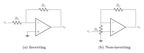
Inverting and non-inverting feedback circuits used in virtual-short derivations.
Inverting amplifier
Section titled “Inverting amplifier”Since , the inverting node is at virtual ground. KCL there gives
so
The minus sign denotes inversion. A bias-current compensation resistor is often placed from to ground.
Non-inverting amplifier and follower
Section titled “Non-inverting amplifier and follower”Here . With negligible input current, the feedback network is an unloaded divider:
The signal is not inverted and input impedance is ideally infinite. Directly connecting output to the inverting input gives the voltage follower, , used to buffer a high-resistance source from a low-resistance load.
Linear Computing Applications
Section titled “Linear Computing Applications”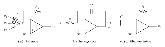
Summing, integrating and differentiating applications.
Summing amplifier
Section titled “Summing amplifier”Applying KCL to the virtual-ground summing node gives
Equal produce a scaled sum; unequal values produce a weighted sum. Applications include audio mixing, level shifting and DACs.
Difference amplifier
Section titled “Difference amplifier”For the standard four-resistor circuit, exact ratio matching gives
Equal common-mode components cancel ideally. Ratio mismatch converts common-mode voltage to differential error and therefore limits circuit CMRR.
Integrator
Section titled “Integrator”With ,
A constant input gives a ramp of slope ; a square wave gives a triangular wave. Because the ideal circuit has infinite DC gain, offsets drive it into saturation. A large resistor parallel to gives a finite low-frequency gain in a practical integrator.
Differentiator
Section titled “Differentiator”The capacitor current flows through , so
A triangular input gives a square output and a step gives a narrow pulse. Since rises without bound, the ideal circuit amplifies high-frequency noise and can become unstable. A practical differentiator adds a series input resistor and a small capacitor across to confine operation to a finite band.
| Circuit | Mathematical action/use | Main limitation |
|---|---|---|
| Summer | Weighted addition; mixers and DACs | Resistor accuracy and output range |
| Difference amplifier | Subtraction/common-mode rejection | Ratio matching determines CMRR |
| Integrator | ; ramps, waveform generation, filters | Offset-driven DC saturation |
| Differentiator | ; edge detection and pulse shaping | Noise gain and high-frequency stability |
Linear op-amp applications and their dominant practical limits.
Types of Op-Amp
Section titled “Types of Op-Amp”| Type | Defining features | Trade-off | Typical use |
|---|---|---|---|
| General-purpose | Balanced gain, speed, offset and cost | No extreme specification | Basic amplifiers and filters |
| High-speed | High GBW/SR, short settling | Power, noise, layout sensitivity | Video, pulse and fast ADC drive |
| Precision | Low offset, drift, bias and noise; high CMRR/PSRR | Often lower speed or higher cost | Bridges and DC measurement |
| Power | High output current/voltage and protection | Heat and large package | Actuators, speakers, supplies |
| Comparator | Fast open-loop switching, logic output | Poor linear-feedback behavior | Threshold/zero crossing |
| Norton | Responds to ; often single supply | Nonstandard input behavior | Current-mode filters/oscillators |
| Instrumentation | High , accurate differential gain/CMRR | Matching and extra amplifiers | Sensor and biomedical signals |
| Isolation | Galvanic input–output barrier | Bandwidth, error and cost | High-side and safety isolation |
Classification by the property optimized.
A comparator may share the triangle symbol but is optimized to switch open loop; an ordinary op-amp used this way may have slow saturation recovery, invalid common-mode inputs or unsuitable output levels. A Norton amplifier forms an input-current difference. An isolation amplifier transfers the signal optically, capacitively or magnetically while maintaining separate grounds; isolation rating, leakage and barrier safety are specifications in addition to gain and bandwidth.
Three-Op-Amp Instrumentation Amplifier
Section titled “Three-Op-Amp Instrumentation Amplifier”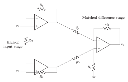
Three-op-amp instrumentation amplifier; one resistor sets first-stage gain.
The two non-inverting input amplifiers buffer both sources. Their inverting nodes are joined by , so the differential current is and each equal feedback resistor contributes gain. The matched final subtractor rejects the buffered common-mode voltage. For the shown ratios,