CMOS (Complementary Metal-Oxide-Semiconductor) Devices
Definition and Structure
Section titled “Definition and Structure”-
Definition: CMOS technology integrates both P-type and N-type enhancement-mode MOSFETs on the same silicon substrate. The two devices operate in a complementary manner to perform logic operations.
-
Basic component: The foundational CMOS logic block is the CMOS inverter, which uses one P-channel MOSFET () and one N-channel MOSFET () connected in series between the supply rails.
-
Terminal connections:
-
Gates: The gates are tied together to form the input terminal , so one input signal controls both transistors simultaneously.
-
Drains: The drains are connected together to form the output terminal , where the inverted logic signal appears.
-
Sources: The P-channel source connects to the positive supply , while the N-channel source connects directly to circuit ground.
-
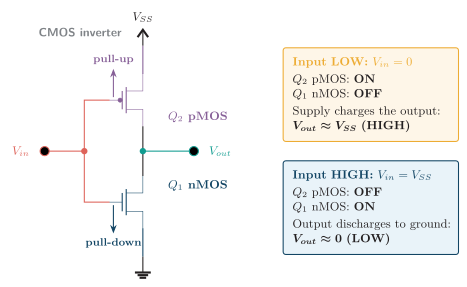
Color-coded CMOS inverter and its complementary switching states.
The physical cross-section shows why CMOS is called complementary. The pMOS device is formed directly in the N-type substrate, while the nMOS device is formed inside a P-type well. The substrate contact is tied to the pMOS source at , and the P-well contact is tied to the nMOS source at ground. These body connections keep the source-body junctions from becoming forward biased during normal operation.
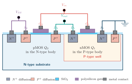
Integrated CMOS inverter cross-section showing the N-type substrate, P-type well, source and drain diffusions, oxide, gates, contacts, and interconnections.
Features and Advantages (With Technical Reasons)
Section titled “Features and Advantages (With Technical Reasons)”High Input Impedance
Section titled “High Input Impedance”-
Why: Each gate is physically isolated from its channel by a non-conductive silicon-dioxide layer (), which blocks steady DC gate current. The input behaves mainly as a capacitance.
-
Application benefit: Negligible DC loading prevents signal loss and permits high fan-out: one logic gate can drive many following CMOS gates. In practice, a larger fan-out increases total input capacitance and therefore slows transitions.
Exceptionally Low Power Consumption
Section titled “Exceptionally Low Power Consumption”-
Why: In either stable logic state, one transistor is ON and the other is OFF. Ideally, the OFF device breaks the direct path from the supply to ground, so essentially no steady-state current flows through the inverter.
-
Application benefit: Low static power makes CMOS highly efficient for battery-powered devices such as smartphones, laptops, digital watches, and embedded systems.
Compact Size (Occupies Less Space Than BJTs)
Section titled “Compact Size (Occupies Less Space Than BJTs)”-
Why: MOSFETs have a comparatively simple planar structure and CMOS logic does not require the bulky, continuously dissipating bias resistors used by many BJT logic circuits.
-
Application benefit: CMOS supports ultra-high-density integration, allowing billions of transistors to be fabricated on a single microprocessor or memory chip.
Technical Limitations
Section titled “Technical Limitations”Switching Delay
Section titled “Switching Delay”-
Why: MOSFET gates and interconnections possess inherent capacitance. This capacitance must be charged or discharged whenever the logic state changes, and the available transistor current is finite.
-
Impact: Propagation delay increases with load capacitance and fan-out. Traditional CMOS can therefore be slower than some current-driven bipolar logic families in demanding high-frequency applications.
Working Principle (CMOS Inverter Operation)
Section titled “Working Principle (CMOS Inverter Operation)”An inverter acts as a logical NOT gate, converting a HIGH input into a LOW output and a LOW input into a HIGH output.
Case 1: Is Logic LOW ()
Section titled “Case 1: VinV_{in}Vin Is Logic LOW (0 V0\,\mathrm{V}0V)”-
P-channel : Since , the pMOS turns ON and provides a low-resistance pull-up path to the supply.
-
N-channel : Since , the nMOS remains OFF and blocks the pull-down path to ground.
-
Output : The pull-up transistor supplies current to the load and charges the output capacitance, raising to approximately , which is logic HIGH. Once an unloaded ideal output is fully charged, its steady-state current becomes zero.
Case 2: Is Logic HIGH ()
Section titled “Case 2: VinV_{in}Vin Is Logic HIGH (VSSV_{SS}VSS)”-
P-channel : Since , the pMOS turns OFF and isolates the output from the positive supply.
-
N-channel : Since , the nMOS turns ON and provides a low-resistance pull-down path to ground.
-
Output : The output capacitance and any load discharge through , pulling down to approximately , which is logic LOW.
| Input | pMOS | nMOS | Output |
|---|---|---|---|
| LOW () | ON | OFF | HIGH () |
| HIGH () | OFF | ON | LOW () |
Thus, in Boolean notation,
Exam Concept: Static vs. Dynamic Power Dissipation
Section titled “Exam Concept: Static vs. Dynamic Power Dissipation”Static Condition
Section titled “Static Condition”In either stable state, one of the complementary MOSFETs is OFF. The ideal path between and ground is therefore broken, so ideal static power dissipation is zero. A real CMOS inverter has small subthreshold, gate-oxide, and reverse-junction leakage currents, giving
Dynamic Condition
Section titled “Dynamic Condition”Power is consumed when the input changes state for two main reasons:
-
The conducting transistor must charge or discharge the total output capacitance .
-
During the brief transition interval, both transistors can be partially ON, creating a short-circuit current pulse from supply to ground.
The dominant first-order capacitive-power relation is
where is the switching-activity factor, is the clock or event frequency, and is the short-circuit component.